
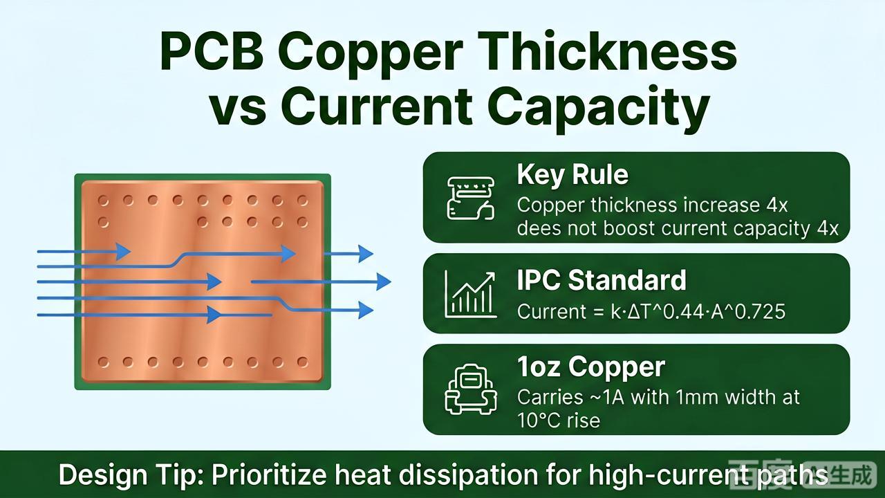
For high-current PCBs, thicker copper foil is not necessarily the most cost-effective choice—quadrupling the copper thickness does not quadruple the current-carrying capacity.
Engineers working on energy storage BMS, inverters, and motor controllers almost invariably face the same question when designing high-current PCB traces: exactly how thick should the copper foil be to ensure cost-effectiveness?
Increasing copper thickness from 1 oz to 2 oz seems reasonable. Moving from 2 oz to 3 oz significantly raises costs while offering only a modest reduction in temperature rise. Going beyond 3 oz, however, leads to doubled quotes from PCB manufacturers, longer lead times, and lower yields—yet the gains in current-carrying capacity become increasingly marginal.
This is not just your imagination. The relationship between copper thickness and current-carrying capacity follows a classic curve of diminishing returns.
By exactly how much does current-carrying capacity increase when copper thickness is raised from 1 oz to 4 oz?
Let’s start with the empirical relationship between copper thickness and current-carrying capacity defined in the IPC-2221 standard. Taking a 10°C temperature rise and an outer-layer trace as an example, the standard’s commonly used empirical formula is: Current (I) ∝ Cross-sectional Area^0.725.
| Copper Thickness | Relative Current Capacity Multiplier (compared to 1oz, calculated by IPC-2221 empirical formula) | PCB Manufacturing Cost Range (compared to 1oz) |
| 1oz (35μm) | 1.0x (baseline) | 1.0x |
| 2oz (70μm) | ~1.65x | ~1.3-1.5x |
| 3oz (105μm) | ~2.2x | ~2.5-3x |
| 4oz (140μm) | ~2.7x | May multiply several times (depending on the PCB manufacturer and process) |
Note: IPC-2221 relies on classic empirical formulas suitable for quick, conservative estimates. IPC-2152 is currently the more valuable reference standard; it employs a current-carrying design method based on extensive empirical data. It accounts for real-world thermal factors—such as board thickness, copper planes, conductor placement, and adjacent conductors—making it more accurate than IPC-2221, though it cannot be summarized by a simple, fixed "multiplier."
This table highlights two key points:
First, the returns on increasing copper foil thickness diminish rapidly. Moving from 1 oz to 2 oz increases current-carrying capacity by approximately 65%; the jump from 2 oz to 3 oz yields only about a 35% increase, and the move from 3 oz to 4 oz adds just 25%. While the absolute gains are somewhat higher than one might expect, the trend of diminishing returns is clear: doubling the copper thickness does not double the current-carrying capacity.
Second, costs rise much faster. 2 oz copper foil costs only 30–50% more than 1 oz, whereas 3 oz foil is 1.5 to 2 times more expensive, and 4 oz foil can cost several times more (depending on layer count, trace spacing, surface area, and order volume). Furthermore, many PCB manufacturers impose minimum order quantity requirements for copper weights exceeding 3 oz, and lead times may be longer.
If you divide the "current-carrying gain per additional ounce of copper" by the "increase in cost," the conclusion remains the same: 2 oz offers the best cost-performance ratio; 3 oz is marginally viable; and anything above 4 oz requires careful cost-benefit analysis.
Why do returns diminish as copper foil gets thicker?
This is not some "black magic" used by PCB manufacturers, but a matter of fundamental physical constraints.Heat dissipation is the primary bottleneck, though the details are complex. A copper trace's current-carrying capacity is limited by temperature rise; for instance, an outer-layer trace that is 1 mm wide and 1 oz thick typically handles current in the range of a few amperes for a 10°C temperature rise. Using 2oz copper does not result in a doubling of capacity under identical conditions because heat dissipation is constrained by the entire thermal path. Heat generated by the current dissipates via multiple routes: direct convection from the copper foil surface, lateral and vertical conduction through the FR-4 substrate, diffusion into adjacent copper pours and power planes, conduction through pads and vias, and convection from board edges and the enclosure. While increasing copper thickness reduces conductor resistance, the PCB's overall heat dissipation capability does not improve proportionally. As copper foil thickness increases, the primary factor limiting current-carrying capacity shifts from conductor resistance to the composite thermal path formed by the FR-4, adjacent copper surfaces, air, and structural components; consequently, the gains in current-carrying capacity do not scale linearly with copper thickness.
Manufacturing limitations. When copper foil exceeds 3oz (105μm), etching precision in PCB manufacturing begins to decline; issues such as undercutting (lateral etching) on fine-pitch traces become severe, and line-width tolerances widen. Traditional empirical models based on IPC-2221 typically apply more conservative current-carrying coefficients to inner layers; however, IPC-2152 indicates that the difference between inner and outer layers depends heavily on board thickness, copper planes, and actual thermal diffusion paths, meaning a simple fixed ratio cannot be applied.
The via bottleneck. High-current applications often require paralleling multiple layers, with vias serving as the bridges between them. However, the copper plating thickness in standard vias is typically around 25μm. Even with multiple vias, their total cross-sectional area remains far smaller than that of the primary traces on the outer layers; thus, the bottleneck for high-current flow often lies not in the copper foil itself, but in the vias.
When should you switch strategies? — The crossover point between copper foil and copper busbars
If the high-current requirements for your PCB traces exceed a certain magnitude, thickening the copper foil is no longer the optimal solution:
| Indicator | Copper Foil Applicable Area | Copper Bar/Copper Row Preferred Area |
| Continuous Current | Lower current levels (e.g., 10-20A) | Start evaluating alternative solutions at 30A level |
| Copper Foil Thickness | ≤2oz (70μm) | Evaluate alternative solutions when ≥3oz |
| Trace Width | ≤12mm | ≥12mm (PCB space starts to become tight) |
| Heat Dissipation Conditions | With air cooling or large-area copper clad | Natural convection or enclosed space |
| Layer Limitations | 4-6 layers can be used in parallel | Bottlenecks appear in multi-layer parallel vias |
The crossover point lies in the 30A range, but it is not a hard dividing line. Whether a design can rely solely on copper foil for 30A depends on a multitude of factors: trace length, permissible temperature rise, allowable voltage drop, copper thickness and trace width, single-layer vs. multi-layer parallel configurations, the presence of large copper pours, the duty cycle of the continuous current, cooling (forced air vs. potting) conditions, and even the current-carrying capabilities of terminals, vias, and solder joints. For instance, carrying 30A over a 10mm trace presents a completely different challenge than doing so over a 200mm trace; a short-duration 60A pulse might actually be easier to manage than a continuous 20A current.
Therefore, a more accurate statement is this: under typical conditions—using FR-4, multi-layer boards, and natural convection cooling—once continuous current reaches the 30A level, or when a 2oz copper trace would require a width of over ten millimeters, it is worth simultaneously evaluating alternatives such as surface-mounted copper strips, embedded copper, or localized copper thickening. 30A is not an absolute threshold, but rather a starting point for engineering assessment.
One alternative is the use of surface-mounted copper strips on the PCB—soldering copper strips or busbars directly onto the board—which allows for a cross-sectional area five to ten times (or more) greater than that of thick copper foil:
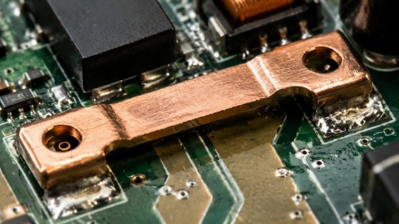
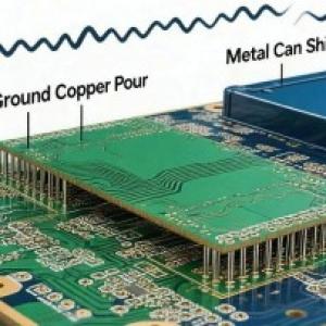
Surface-mount copper strips are soldered onto the PCB; their cross-sectional area is far greater than that of thick copper foil traces.
| Solution | Equivalent Cross-sectional Area | PCB Cost (relative to 2oz baseline) | Assembly Complexity |
| 2oz copper foil, 12mm wide | ~0.84mm² | Baseline | None |
| 3oz copper foil, 12mm wide | ~1.26mm² | +150% | None |
| 1.5×2mm copper bar | ~3.0mm² | +5-15% | Requires welding |
| 2×3mm copper bar | ~6.0mm² | +10-20% | Requires welding |
The data above serves as an illustrative comparison and does not represent a universal current-carrying rating. Actual temperature rise depends on trace length, copper strip material, pad heat dissipation conditions, ambient temperature, and mounting orientation; it cannot be determined solely by cross-sectional area.
In terms of cross-sectional area, a 2×3mm copper strip (6.0mm²) has an area approximately 7.1 times that of a 2oz, 12mm-wide trace (0.84mm²)—equivalent to the cross-section of a 12mm-wide, ~14oz copper conductor, a specification that is virtually impossible to achieve in standard PCB manufacturing.
A practical design decision-making process
Step 1 — Calculate requirements. Determine the continuous current, as well as the allowable temperature rise and voltage drop. Do not use peak current values to calculate copper foil requirements; many design issues actually stem from miscalculating the operating conditions.Step 2 — Determine if copper foil suffices. Use IPC-2152 (more accurate) or IPC-2221 curves (for quick estimation) to check if 2oz copper foil at a reasonable width is feasible. If a trace width exceeding 12mm still fails to keep the temperature rise within limits, or if the voltage drop exceeds design requirements → Proceed to Step 3.
Step 3 — Evaluate 3oz or heavier copper options. While 3oz copper foil is feasible, costs increase by 1.5 to 2 times, lead times may extend, and etching precision decreases. If the total copper cost exceeds the price difference of alternative solutions → Proceed to Step 4.
Step 4 — Adopt a copper strip solution. Reserve pads on the PCB to solder on surface-mount copper strips, busbars, or terminals. From this point on, current-carrying capacity is no longer primarily limited by copper foil thickness, but rather by the copper strip's cross-sectional area and the quality of the solder joint.
Three commonly overlooked points
1. Copper strips offer superior heat dissipation compared to copper foil. Copper strips protrude from the PCB surface, allowing for convective cooling on all sides. In contrast, copper foil is either encased in FR-4 (inner layers) or exposed on only one side (outer layers), which restricts heat dissipation paths. For similar cross-sectional areas, copper strips protruding from the PCB surface generally offer more favorable conditions for convective heat dissipation; however, the actual performance gain depends on factors such as the strip's shape, pad design, soldering quality, and the system's overall thermal environment, requiring evaluation based on the specific design.2. Don't miscalculate the costs associated with copper foil versus copper strips. A PCB using 4 oz copper foil can cost several times more than one using 2 oz foil and requires a higher-tier manufacturer; the exact price multiplier depends on the manufacturer's quote and DFM (Design for Manufacturability) results. In contrast, the material cost for a surface-mount copper strip is merely a fraction of a yuan, and the soldering process is integrated into the standard SMT reflow cycle, requiring no additional manufacturing steps.
3. Ensure the pad design is adequate. Copper strips connect to the PCB via pads, and the copper foil area of the pad must be sufficiently large to facilitate effective heat transfer. Many copper strip implementations fail not because the strip itself is undersized, but because undersized pads result in excessive thermal resistance after soldering—causing a significant temperature rise at the solder joint even while the copper strip itself remains relatively cool.
Conclusion
Copper foil is the most cost-effective choice up to a thickness of 2 oz; 3 oz is feasible but borderline; beyond 3 oz, a copper busbar solution should be seriously evaluated.This is not a simple case of one replacing the other—both copper foil and copper busbars have their own optimal application ranges. Copper foil is suitable for lower currents (in the 10–20 A range), but once you reach the 30 A level—where the trade-offs become critical—it is worth considering a copper busbar solution alongside it. Understanding the crossover point between the two is key to an engineer's ability to make the right design choices for high-current PCBs.
The next time you face the question of "how thick the copper foil needs to be," start by calculating whether your current has crossed that threshold.