
What is the standard for PCB warpage? What causes PCB warpage?
PCB is also known as printed circuit board, any one of the electronic products have PCB in the role. To improve your knowledge of PCB, this article will be introduced to PCB warpage, PCB warpage standards and the causes of warpage in the PCB processing. If you are interested in PCB or the contents of this article, you may wish to continue reading down with the editor.First, what is PCB warpage?
In order to correctly place the SMT components, the PCB must remain completely flat. For accurate placement, the placement machine must release the SMT components to the same height above the board for all components.
If the PCB is warped, i.e. not flat, the machine will not be able to maintain a constant height when releasing the components as they are placed on the board - this can affect placement accuracy, especially for fine pitch components.
In addition, flat PCBs help to keep the SMT components in the right position during reflow. If the high temperatures in the reflow oven cause changes in board flatness, SMT components can slip out of position as they float on the molten solder, leading to solder bridging and open circuits.
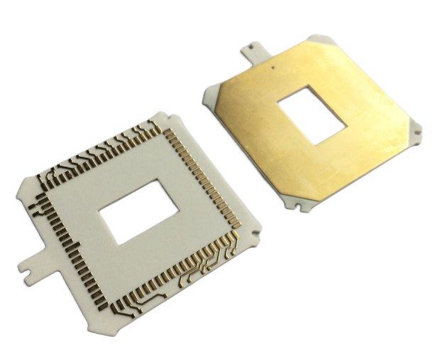
PCBs are usually made of glass fibre and some other composite materials and most are laminated only once and are very simple.
PCB warpage is a change in the shape of the PCB.
Second, what is the standard for PCB warpage?
According to IPS standards, the warpage (WD) of the PCB to be mounted should be less than or equal to 0.75%. In other words, when the WD is greater than 0.75%, it should be judged as a warped board, or defective product.
In fact, in the case of not mounting components but only the need for inserts, the board flatness requirements are even lower and the WD standard can be less than or equal to 1.5%.
Of course, some manufacturers in order to meet higher customer demand, they can pursue more stringent standards, some WD standards need to be less than or equal to 0.5%, or even this requirement to less than or equal to 0.3%.
Third, the PCB processing process causes warpage
The causes of PCB processing warpage are complex and can be divided into thermal and mechanical stresses.
Among them, thermal stress is mainly generated in the pressing process, mechanical stress is mainly in the stacking of plates, handling and baking process.
1) PCB warpage caused by the incoming laminate process
Laminates are double-sided, symmetrical structure, no graphics. The CTE of copper foil and glass cloth is almost the same, so there is almost no warpage caused by different CTE during the pressing process.
However, the size of the laminate press is large and temperature differences in different areas of the hot plate can lead to slight differences in the curing rate and degree of cure of the resin in different areas of the press-fit process. There are also large differences in dynamic viscosity at different rates of temperature rise and therefore also local stresses due to differences in the curing process.
Generally this stress will remain in equilibrium after pressing, but will be gradually released and deformed in the subsequent processing.
2) PCB warpage caused by the PCB stack-up process
PCB stack-up process is the main process to generate thermal stress. Similar to the laminate stack, also due to differences in the curing process and local stress. Due to the thicker thickness, varied pattern distribution and more prepreg, thermal stresses can be more difficult to eliminate than in copper-clad boards.
The stresses in the PCB board are released during the subsequent drilling, forming or grilling process, resulting in board distortion.
3) PCB warpage caused by solder resist layer and screen printing baking process
As solder resist inks cannot be stacked on top of each other during the curing process, the PCB board will be placed in a rack to bake the board to cure.
The solder resist temperature is around 150°C, which exceeds the Tg value of the laminate and the PCB tends to soften resulting in failure to withstand high temperatures. The manufacturer must heat both sides of the substrate evenly, while keeping the processing time as short as possible to reduce warpage of the substrate.
4) PCB cooling and heating process caused by the PCB warpage
Solder furnace temperature 225 ℃ -265 ℃, ordinary board hot air solder leveling time 3s-6s. hot air temperature of 280 ℃ -300 ℃.
After solder levelling, the board is put into the tin furnace from room temperature and is washed with room temperature post-treatment water within two minutes after discharge from the furnace. The entire hot air soldering and levelling process is a process of sudden heating and cooling.
Due to the different materials and uneven structure of the board, thermal stresses will inevitably occur during the cooling and heating process, resulting in micro-strain and overall deformation of the warped area.
5) PCB warpage caused by improper storage
PCB boards in the semi-finished stage of storage, are generally firmly inserted in the shelves, the shelves are not adjusted for elasticity, or the stacking of the board during storage can lead to mechanical deformation of the board.
Especially thin boards below 2.0mm are more seriously affected.


