Fundamentals of PCB EMC Design: Key Techniques to Ensure the Board Is Neither Radiative nor Susceptible
EMC (Electromagnetic Compatibility) is one of the most troublesome areas for hardware engineers. Unlike impedance calculations, it doesn't have explicit formulas, nor does it have clear checklists like routing rules. EMC problems are often the result of multiple factors combined, and troubleshooting is like "whack-a-mole"—plug one hole, and two more pop up.But EMC isn't some mystical concept. Over 70% of EMC problems are determined during the PCB schematic and layout stages. No matter how much troubleshooting is done later, it's just filling in the holes dug earlier. This article will discuss grounding, return paths, decoupling filtering, and shielding.
- Basic EMC Concepts – Radiation and Immunity, Common Standards
- Grounding Design – Single-Point Grounding, Multi-Point Grounding, Advantages and Disadvantages of Ground Plane Segmentation
- Return Path – The Nature of Signal Return Current, Loop Area Control
- Decoupling and Filtering – Decoupling Capacitor Selection and Placement, EMI Filtering Strategies
- Shielding Techniques – Via Barriers, Copper Shielding, Metal Covers
- My EMC Design Checklist
EMC (Electromagnetic Compatibility) encompasses two aspects:
- EMI (Electromagnetic Interference)
—The electromagnetic noise emitted by equipment must not exceed standard limits (radiated emissions, conducted emissions).
- EMS (Electromagnetic Susceptibility)
—The ability of equipment to function normally under certain electromagnetic interference environments (ESD, surge, electrical fast transient/burst, etc.).
In other words, EMC requires that your board neither interferes with others (EMI compliance) nor is interfered with by others (EMS compliance).
1.1 How common are EMC problems?
Let me share a few real-world examples from my personal experience.
Case 1: An industrial control board passed all functional tests but was sent for CE certification radiation testing. It exceeded the limit by 15dB at 30MHz. After two weeks of investigation, it was found that the switching noise of the DC-DC power supply was radiating through the power line. Adding a π-type filter and a ferrite bead to the DC-DC input reduced the radiation by 20dB, and the board passed on the first try.
Case 2: A vehicle camera module reset upon ESD at ±4kV. After extensive investigation, it was found that the USB interface's GND was not directly connected to the chassis ground, allowing static energy to accumulate and impact the chip's I/O. Changing the grounding method easily resolved the ±8kV issue.
Case 3: A communication base station's RF board exceeded the radiation limit at 1.2GHz. Initially, it was thought to be a problem with the RF power amplifier, but it turned out to be the 9th harmonic of the FPGA clock (125MHz). Adding a spread spectrum to the FPGA clock reduced the radiation by 12dB.
These three cases share a common thread: the boards all functioned correctly, and the EMC issues only surfaced during the certification phase. Once this stage is reached, the rectification period can easily take one or two months, and in some cases, it may even require redesigning the entire board. Therefore, my principle is: EMC should be considered during the design phase, not wait until problems arise before making changes.
1.2 The Essence of EMC Issues
Remember this formula; all subsequent EMC countermeasures can be explained using it:
Radiation intensity ∝ Frequency² × Current × Loop area
The higher the frequency, the stronger the radiation, making high-speed clocks the number one enemy of EMC. The larger the current, the stronger the radiation, making power switching transistors and high-current drivers key monitoring targets. However, for those of us in PCB design, the third factor we can truly control is loop area. The grounding, return current, decoupling, and shielding discussed later all ultimately do the same thing: minimize loop area.
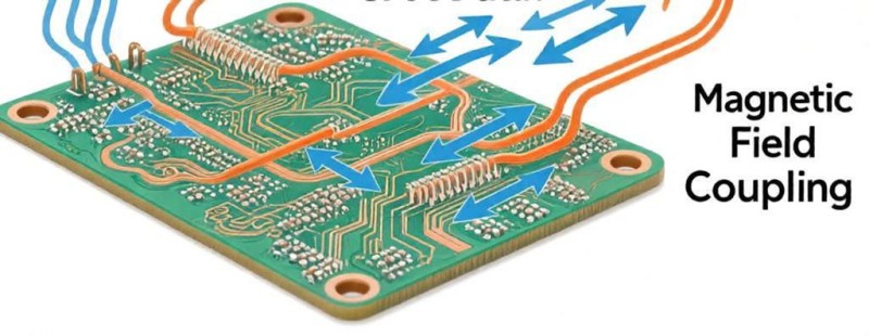
▲ Common EMC coupling mechanisms on PCBs
Some experience:
Simply put, EMC is about controlling where electromagnetic energy flows. It's about retaining what needs to be retained (EMI) and blocking what needs to be blocked (EMS). At the PCB level, what you can do is: reduce loop area, provide a low-impedance return path for the current, and cut off coupling paths. Doing these three things will solve a large part of the EMC problem.
1.3 Common EMC Test Items
Test Item
Category
Typical Standard
PCB-level Countermeasures
Radiated Emission (RE)
EMI
CISPR 32/EN 55032
Loop reduction, filtering, shielding
Conducted Emission (CE)
EMI
CISPR 32/EN 55032
Power supply filtering, decoupling optimization
Electrostatic Discharge (ESD)
EMS
IEC 61000-4-2
Grounding, TVS diode, trace protection
Radiated Susceptibility (RS)
EMS
IEC 61000-4-3
Shielding, filtering, differential transmission
Surge
EMS
IEC 61000-4-5
TVS diode, gas discharge tube
Electrical Fast Transient (EFT)
EMS
IEC 61000-4-4
Filtering, ferrite bead, decoupling
II. Grounding Design: The Foundation of EMC
Grounding is the most important and error-prone aspect of EMC design. There's a saying in the EMC world: "If you can only do one thing to improve EMC, improve grounding." This is no exaggeration.
Why is grounding so important? Because all EMC problems ultimately boil down to "current having nowhere to go" or "current taking the wrong path." A good grounding system provides a low-impedance return path for current, reducing loop area and lowering radiation.
2.1 Three Basic Grounding Methods Traditionally, there are three grounding methods: single-point grounding, multi-point grounding, and hybrid grounding.
Single-Point Grounding: The ground wires of all circuits converge at a single point. The advantage is that the ground currents between circuits do not interfere with each other, and there is no common ground impedance coupling. The disadvantage is that the ground wire inductance is large at high frequencies, making it unsuitable for circuits above 10MHz.
Applicable Scenarios: Low-frequency analog circuits (audio, sensor signal conditioning); single-point grounding is suitable for frequencies <10MHz.
Multi-Point Ground: The circuit is grounded as close as possible to the nearest point, achieving low-impedance connections at each point through a large ground plane. Advantages include low ground impedance and low radiation at high frequencies. Disadvantages include the potential for ground loops and susceptibility to ground noise interference at low frequencies.
Suitable for: High-frequency digital circuits and high-speed signals (>10MHz), the mainstream method in modern PCBs.
Hybrid Ground: Single-point grounding for low frequencies and multi-point grounding for high frequencies. Frequency-dependent ground switching is achieved through capacitors or inductors—capacitors exhibit high impedance at low frequencies (single-point grounding effect) and low impedance at high frequencies (multi-point grounding effect).
Suitable for: Mixed-signal boards containing both low-frequency analog and high-frequency digital signals.
2.2 Ground Plane Design on PCBs
In modern multilayer PCB design, the core principle of proper grounding is maintaining a complete ground plane.
A complete ground plane without arbitrary divisions or large gaps forms a current return path with extremely low impedance, making it the most practical and cost-effective design method for solving EMC problems.
How low is the impedance of a ground plane? Let's take a real-world example: On a standard 1.6mm thick FR-4 four-layer PCB, with the second layer entirely covered as ground, at a 100MHz operating frequency, the AC impedance of a 1cm square ground plane is only a few milliohms. In contrast, a 10cm long ordinary signal trace at the same frequency can have an impedance of tens of ohms—a difference of thousands of times.
2.3 Ground Plane Segmentation: Be Cautious!
Many engineers like to divide the ground plane into "analog ground" and "digital ground," believing this isolates noise. This can be effective on low-frequency boards, but on high-speed boards, it often makes things worse.
On some boards, even with complete separation of analog and digital grounds, actual measurements show that radiation is actually higher than without separation. The reasons are simple:
- When a signal crosses a slot, the return current is forced to take a large detour, multiplying the loop area several times over and increasing radiation exponentially.
- When a signal passes the slot boundary, the characteristic impedance changes abruptly, causing reflection.
- The slits formed by the slots can resonate like antennas at certain frequencies, turning the intended noise isolation into a radiation source.
My suggestion is: prioritize keeping the ground plane intact on mixed-signal boards and avoid unnecessary slotting. If you must slot, pay attention to the following: connect analog and digital grounds at a single point below the ADC/DAC chip; never allow high-speed signals to cross slots (if they do, place a bridging capacitor on the slot); keep slots as short as possible; long slots act as antennas; and create a via fence around the slotted area to lock in energy.
Some experience:
My rule of thumb is simple: avoid splitting if possible. A complete ground plane is the best insurance for EMC. When should you consider splitting? In scenarios with very low signal frequencies (<1MHz) and extreme noise sensitivity (precision ADCs, microvolt sensors). Even if you do split, ensure that signals in the analog and digital areas do not cross boundaries.
III. Return Path: The Core of EMC
I've noticed many people understand it this way: a signal starts from the transmitter, travels along the trace to the receiver, and transmission is complete. However, in reality, a signal is a closed loop. Current flows from the transmitter, reaches the receiver, and must return to the transmitter via a certain path. This return path is called the return path.
The return path determines the signal loop area, and the loop area directly determines the radiation intensity. This is the most core concept in PCB-level EMC design.
3.1 Which Path Does the Return Current Take?
A basic physical law: the return current automatically chooses the path of lowest impedance. For low-frequency signals (<100kHz), "lowest impedance" means "lowest resistance"—the return current takes the shortest geometric path. But for high-frequency signals (>1MHz), "lowest impedance" means "lowest inductance"—the return current will flow close to the reference plane below the signal trace, even if this path's geometric distance isn't the shortest.
The physical essence of this phenomenon is that the signal trace and the return path below it form a transmission line pair. When current flows to the right on the signal line, the return current flows to the left on the ground plane. The closer the two are, the smaller the loop area, the lower the inductance, and the lower the impedance.
The distribution of the return current on the ground plane also follows a pattern—at high frequencies, the return current is concentrated on both sides of the signal line within a range of three times the dielectric thickness. The higher the frequency, the more concentrated the return current is directly below the trace.
3.2 Loop Area Control
Radiation intensity is proportional to the loop area. Therefore, one of the core goals of EMC design is to minimize the signal loop area as much as possible.
Under what circumstances will the loop area expand? I've encountered these most often:
- The ground plane is slotted, forcing the signal to cross it;
- The reference plane changes when the signal changes layers (e.g., from GND to Power);
- The signal layer is too far from the reference plane in the layer stack design;
- There are too few GND pins on the inter-board connectors.
The first one is the most common.
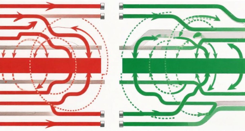
▲ Comparison of return paths: On the left, the signal crosses the ground plane segmentation slot, forcing the return path to detour and drastically increasing the loop area;
on the right, the ground plane is intact, and the return path runs close to the underside of the cable.
3.3 Return Current Handling for High-Speed Signal Layer Changes
In the previous routing article, I mentioned the need for return current vias (Stitching Vias) during high-speed signal layer changes. Here, I'll emphasize this again from an EMC perspective.
Suppose a signal changes from L1 (microstrip line, referencing the GND plane of L2) to L4 (stripline, referencing the GND plane of L3). The vias themselves are fine, but what about the return current? The return current needs a path to jump from the GND plane of L2 to the GND plane of L3. Without return current vias, the return current has to detour from a very far location, forming a huge loop.
Layer Switching Return Current Rules:
1. If the reference plane is the same before and after the layer switch (both are GND), place 1-2 GND vias next to the layer switch via.
2. If the reference plane is different before and after the layer switch (from GND to Power), place a decoupling capacitor (0.1μF) at the layer switch location, bridging GND and Power.
3. Both lines of the differential pair must switch layers simultaneously to ensure symmetrical return current.
3.4 Common Impedance Coupling
When two circuits share a ground or power line, the voltage drop generated by the current in one circuit across the common impedance will couple to the other circuit—this is common impedance coupling.
For example: A digital chip has a transient current of 500mA, and the ground impedance is 0.1Ω. The voltage noise generated on the ground line is 50mV. This 50mV noise will be directly coupled to the analog circuit sharing the same ground line.
Methods to resolve common impedance coupling:
- Use a complete ground plane to reduce the common impedance to the milliohm level.
- Place decoupling capacitors near high-current devices (FPGA, CPU, DC-DC) to keep transient currents within their local loops.
- Separate layouts for analog and digital circuits to reduce shared paths.
- Widen power supply traces to reduce power path impedance.
Some experience: I encountered a situation where the ADC sampling value kept fluctuating regularly, and filtering couldn't eliminate it. It turned out that transient currents generated by the FPGA's I/O switching were coupled to the ADC's reference voltage through the common ground impedance. After connecting the FPGA and ADC grounds at a single point below the ADC, the noise immediately disappeared. Common impedance coupling is the number one killer of mixed-signal boards; at least one-third of the EMC problems I've encountered are related to it.
IV. Decoupling and Filtering: Two Powerful Tools for EMC
Decoupling and filtering are, in my opinion, the two most practical EMC methods at the PCB level. Decoupling manages internal board issues, providing clean power to the chips and preventing transient currents from running rampant. The filter tube is responsible for the interaction between the board and the external environment, preventing noise from escaping through cables and preventing external noise from entering through cables.
4.1 The Essence of Decoupling Capacitors When digital chips are operating, I/O switching generates huge transient currents. For example, an FPGA with 100 I/Os switching simultaneously, each I/O generating a transient current of 10mA, would have a total transient current of 1A. This 1A current pulse needs to be provided within nanoseconds. However, the power supply module (VRM) is far away and has a slow response time, making it impossible to provide this power in time.
The role of decoupling capacitors is to act as the chip's "local power reserve." Normally, the capacitor charges from the power supply; when the chip needs transient current, the capacitor discharges within nanoseconds to provide energy.
The essence of decoupling capacitors is to reduce the loop area of transient current. Without decoupling capacitors, transient current draws power from the distant power supply module, resulting in a large loop area; with decoupling capacitors, the transient current forms a small loop between the chip and the capacitor, significantly reducing radiation.
4.2 Decoupling Capacitor Selection
Decoupling capacitors cannot be simply "any 0.1μF capacitor will do." Different capacitance values cover different frequency ranges.
| Capacitance | Effective Frequency Range | Typical Package | Application Scenario |
| 10μF | DC ~ Hundreds of kHz | 0805/1206 | Board-level large-capacity energy storage |
| 1μF | Hundreds of kHz ~ 5MHz | 0603/0805 | Intermediate frequency decoupling |
| 0.1μF | 5MHz~200MHz | 0402/0603 | Most commonly used high-frequency decoupling |
| 0.01μF | 200MHz~500MHz | 0402/0201 | High-speed digital decoupling |
| 100pF | 500MHz ~ 2GHz | 0402/0201 | RF / ultra-high-speed decoupling |
Note: The self-resonant frequency (SRF) of a capacitor determines the highest frequency it can cover. Beyond the SRF, the capacitor ceases to be a "capacitor" and becomes an "inductor," drastically reducing its decoupling effect. Small-value capacitors (such as 100pF or 0.01μF) have higher SRFs and can cover higher frequencies.
In practical designs, multiple capacitors of different values are typically placed in parallel near the chip's power supply pins: 10μF + 0.1μF + 0.01μF, covering the entire frequency band from low to high frequencies. This is called multi-capacitor parallel decoupling.
4.3 Decoupling Capacitor Placement The placement of decoupling capacitors has a significant impact on EMC. The core principle is: the closer the capacitor is to the chip's power supply pin, the better, and the shorter the trace, the better.
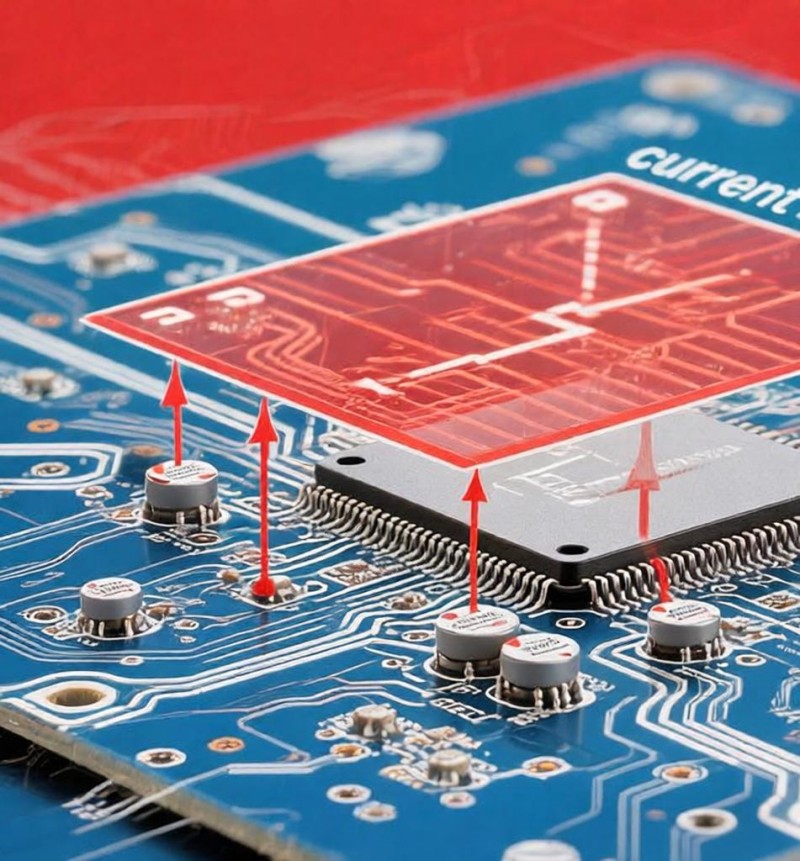
▲ Decoupling capacitors should be placed correctly: close to the IC power pins, with the shortest possible trace length.
How to place them? Here are a few key points:
- Place the vias first, then run the traces. Place the vias on or very close to the pads (<1mm). Avoid the practice of extending the traces first and then placing the vias.
- Power and ground vias should be placed symmetrically on either side of the pads to minimize return loops.
- The length from the power pin to the decoupling capacitor copper trace should be ≤1.5mm, the shorter the better.
- 10μF energy storage capacitors can be slightly further away; all high-frequency decoupling capacitors of 0.1μF and below should be placed close to the pin, without exception.
- Do not connect other traces between capacitors and ICs, especially for high-speed signals.
4.4 EMI Filtering Strategies
Decoupling solves internal board noise, while filtering solves the problem of internal board noise propagating outwards and external noise entering the board. Common EMI filtering measures:
Power Input Filtering
The power input is the main channel for conducting noise in and out. Commonly Used Filtering Structures:
- π-type filter: Capacitor-inductor-capacitor (CLC), suitable for differential-mode noise, with good suppression effect.
- Common-mode inductor: Excellent suppression of common-mode noise (20-40dB), differential-mode signals are almost unaffected.
- Ferrite beads: Exhibit high impedance (tens to hundreds of ohms) at high frequencies, effectively suppressing high-frequency noise (ferrite beads cannot be abused in high-current DC main circuits, as there is voltage drop in DC and severe heat generation with high current).
- Signal Line Filtering: Signal lines from board-side connectors (such as USB, Ethernet, serial ports) are weak points in radiation and immunity:
- RC filter: Resistor + capacitor, suitable for low-speed signals (<1MHz), simple and effective.
- LC filter: Inductor + capacitor, suitable for intermediate frequency signals (1-100MHz), care should be taken not to cause signal ringing.
- ESD protection device: TVS diode, placed at the connector entrance to discharge electrostatic energy to ground.
- Clock Signal Filtering: Clocks are the number one source of EMC radiation. Besides adding small resistors (22Ω for normal clocks, 10~22Ω for high-speed differential clocks) and matching resistors in series on the clock lines:
- Spread Spectrum: If the chip supports it, enable spread spectrum to distribute clock energy across a wider frequency band, reducing peak radiation.
- Reduce Clock Frequency: If performance allows, reducing the clock frequency is the most direct method.
- Ensure a complete ground plane under the clock trace: There must be no slots.
A word of advice: Don't be lazy when using decoupling capacitors. "Placing a 0.1μF capacitor next to each power pin" is just a basic requirement. The real determining factor is trace length. A 0.1μF capacitor with a 10mm trace is less effective at high frequencies than a 0.01μF capacitor with a 1mm trace.Why? Because the extra 9mm of trace parasitic inductance negates the capacitor's high-frequency decoupling capability. So don't worry about the capacitance value; prioritize ensuring the trace is short enough.
V. Shielding Technology: The Last Line of Defense Even with grounding, return current, and filtering in place, what if EMC issues aren't completely resolved? Then physical methods are needed: shielding.
Shielding, simply put, is using conductive materials to trap (or block) electromagnetic energy, similar in principle to a Faraday cage. You can use shielding to prevent internal noise from radiating outwards or to prevent external noise from interfering with internal circuitry.
5.1 PCB-Level Shielding Technology
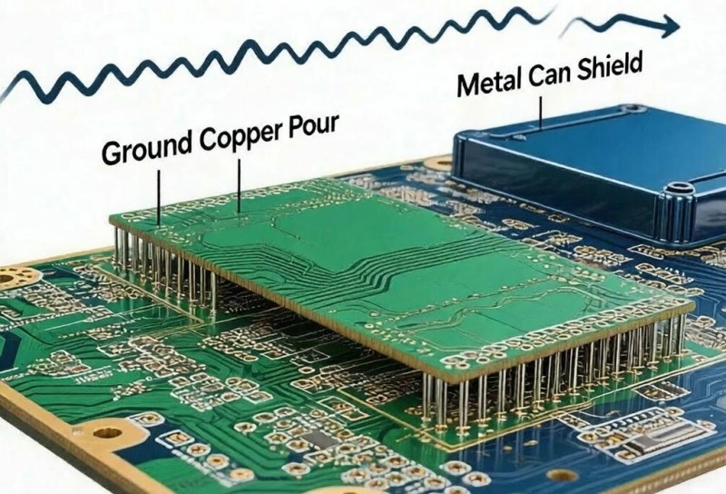
▲ PCB shielding technologies: via barriers, copper shielding, metal covers
There are three commonly used shielding methods at the PCB level:
1. Via Fence: A dense ring of ground vias is placed around sensitive circuits or noise sources. The spacing (strong shielding: via spacing < λ/20; ordinary ground fence: spacing < λ/10, where λ is the wavelength of the highest interference frequency) forms an "electromagnetic barrier" inside the PCB, limiting electromagnetic energy leakage from one area to another.
Typical applications: Isolating high-speed digital and analog areas, isolating clock and RF circuits, and suppressing edge radiation.
2. Copper Shielding: Ground copper is laid on the top or bottom layer to "cover" sensitive circuits. The copper is connected to the ground plane through vias, forming a simple shielding cavity.
Precautions: The copper should not form a closed ring to avoid antenna effects; the via spacing on the copper should be < λ/10 to ensure effectiveness at high frequencies.
3. Metal Can Shielding: A metal can is soldered or clipped onto the PCB to enclose the entire sensitive area. This is the most powerful shielding method, providing shielding effectiveness of 40-60dB or more.
Typical Applications: RF front-ends (WiFi, Bluetooth, cellular), high-speed SerDes areas, emergency measures during EMI rectification.
Key Design Considerations: Sufficient grounding pads should surround the metal can, with pad spacing <λ/20; there should be no suspended traces inside the metal can; openings in the metal can (for heat dissipation and ventilation) should be as small as possible.
5.2 Trace Shielding: For particularly sensitive traces (such as precision analog signals) or particularly noisy traces (such as clock lines), grounded copper foil can be laid on both sides of the trace to form a "coplanar waveguide" structure, essentially giving the trace a "shielding coat."
Trace Shielding Rules:
- The shielding copper trace should be at least 1-2 times the trace width away from the trace; too close will affect impedance.
- The shielding copper trace should be connected to the ground plane via dense vias (spacing < 5mm).
- Differential signals generally do not require trace shielding because differential pairs themselves have good anti-interference capabilities.
5.3 Edge Radiation Suppression
The edge of the PCB is a major source of EMC problems. Trace traces, copper traces, and components along the edge all generate radiation. Methods to suppress edge radiation:
- Use grounding vias around the edge—create a ring of grounding vias around the PCB with a spacing < λ/20, forming an "electromagnetic wall."
- Narrow the power/ground copper traces around the edge—do not extend the power and ground copper traces to the edge; indent them by at least 20mil and connect them to the internal plane vias.
- Keep clock traces away from the edge—maintain a distance of at least 5mm.
- Do not place sensitive components near the edge—keep high-frequency ICs, crystal oscillators, and DC-DC converters away from the edge.
Experience Reminder: Shielding is a last resort, not a first choice. If the problem can be solved at the source, don't rely on shielding as a fallback. If an EMC issue requires a metal shield to resolve, it likely indicates room for improvement in the initial design. A metal shield increases cost and weight, and also complicates heat dissipation. However, when a product is nearing market launch and time is tight, adding a metal shield is indeed the quickest way to "stop the bleeding"—I've done this several times myself.
VI. Practical Rules for PCB Layout EMC EMC problems are rarely caused by a single factor, but rather are the result of multiple factors including layout, routing, grounding, and filtering. Below are my summary of practical EMC rules for PCB layout, arranged in order of design flow:
6.1 Component Layout Rules
1. Functional Zoning – Divide the board into high-speed digital areas, low-speed analog areas, power supply areas, RF areas, etc., maintaining physical distance between areas.
2. Keep Noise Sources Away from Sensitive Circuits – Keep DC-DC converters, crystal oscillators, and FPGAs away from ADCs, RF front-ends, and sensors.
3. Place High-Speed Components Near the Board Center – Keep them away from the board edges to reduce edge radiation.
4. Place Connectors at the Board Edges – Place I/O connectors at the edges of their corresponding zones to shorten the paths for incoming and outgoing signal lines.
5. Place Clock Components Near the User – Place crystal oscillators and clock buffers near the ICs that require clock signals to shorten clock trace lengths.
6.2 EMC Rules for Trace Routing
1. Keep clock traces shortest—clock traces are the largest source of radiation; keep them as short and direct as possible, avoiding detours.
2. Use inner layers for high-speed signals—strip lines (inner layer traces) have two reference planes, resulting in approximately 10dB lower radiation compared to microstrip lines (outer layer traces).
3. Avoid traces forming antennas—trace lengths should not exceed 1/20 of the signal wavelength (approximately 15cm at 100MHz).
4. Avoid large ungrounded copper areas—large areas of ungrounded copper can become parasitic antennas.
5. Prioritize differential signals—use differential transmission whenever possible, as it results in 20-40dB lower radiation compared to single-ended signals.
6.3 Power Integrity Rules
1. Use a complete power plane – the power plane and ground plane are adjacent (dielectric thickness ≤ 0.1mm) to form a low-impedance planar capacitor.
2. Widen high-current power traces – reduce voltage drop and heat generation, and also reduce trace inductance.
3. DC-DC switching noise isolation – lay a ground copper layer under the DC-DC converter, surround it with vias, and add π-type filtering at the input and output.
4. LDO isolation for analog power – the analog chip's power supply is powered separately by an LDO, isolated from the digital power supply.
VII. My EMC Design Checklist
After routing is complete, in addition to the routing checklist in the previous article, you should also run a specific EMC check:
Grounding Check
1. Is the ground plane complete? Are there any unnecessary splits?
2. Are the analog ground/digital ground connection points below the ADC/DAC?
3. Are there grounding vias on the board edge?
4. Are there enough GND pins for all connectors (at least one GND pin for every 3-4 signal pins)?
Return Path Check
1. Do all high-speed signals have a complete reference plane? 2. Are there any signals crossing ground plane segments? If so, have they been bridged?
3. Are there return vias at high-speed signal layer transitions?
4. Is a complete ground plane maintained beneath the clock trace?
Decoupling and Filtering Check
1. Do all IC power pins have decoupling capacitors? Do the capacitance values cover the required frequency range?
2. Are the decoupling capacitors flush with the IC pins? Is the trace length <2mm?
3. Is there EMI filtering (common-mode inductor/π-type filter) at the power input?
4. Are there ESD protection devices at external connector inputs?
5. Are there filter capacitors and ferrite cores at the DC-DC input and output?
Layout and Shielding Check
1. Are high-speed devices kept away from the board edge?
2. Are noise sources (DC-DC, crystal oscillator) kept away from sensitive circuits?
3. Is the clock trace the shortest possible length? Is it kept away from the board edge and I/O connectors?
4. Are there via barriers or copper shielding in sensitive areas?
Note: The checklist is just the passing grade, not the end goal. What truly uncovers problems are simulations and actual measurements. During the design phase, at least run signal integrity and power integrity simulations for critical high-speed signals. If possible, scan the board with a near-field probe upon arrival to expose radiation points early. Many designs that seem "okay" during the design phase turn out to have serious problems in the EMC lab. EMC remediation costs can range from tens of thousands to hundreds of thousands of dollars; this cost must be carefully calculated.
VIII. In Conclusion
EMC is, in my opinion, the most easily overlooked and most expensive aspect of PCB design to remediate. When projects are on tight deadlines, EMC is often the first thing sacrificed; then, it's the first problem to surface in the certification lab.
This article is quite long, but the core message is essentially: radiation intensity is proportional to loop area.
Everything you do—keeping the ground plane intact, changing layers and adding return vias, placing decoupling capacitors close to chips, and adding grounding vias to the board edge—ultimately reduces loop area. Understanding this provides direction for EMC design.
If we must prioritize: first ensure grounding and return current are working correctly (this will solve more than 50% of EMC problems), then optimize decoupling and filtering, and only consider shielding as a last resort.