KEY TECHNOLOGY(HK)CO. ,LIMITED
  • Home
  • Products
    • PCBA
    • Rigid PCB
    • HDI PCB
    • Rigid Flex PCB
    • Flex PCB
    • High Frequency PCB
      • Rogers PCB
      • Isola PCB
      • Arlon PCB
      • Nelco PCB
      • Taconic PCB
      • Teflon PCB
      • Neltec PCB
    • Metal Core PCB
      • Aluminium PCB
      • Copper PCB
    • Ceramic PCB
    • Laser Stencil
    • Reverse engineering
    • Purchasing components
  • Capability
    • PCBA capability
    • Rigid PCB capability
    • HDI PCB Capability
    • Rigid Flex PCB Capability
    • Flex PCB Capability
    • High Frequency PCB Capability
    • Metal Core PCB Capability
    • Ceramic PCB Capability
  • Equipment
    • PCB Equipment
    • PCBA Equipment
  • About us
  • Blogs
  • Inquiry
  • Contact us

Blogs

  1. Home
  2. Blogs
  3. Cell Phone (Mobile phone) HDI PCB PROCES...

Cell Phone (Mobile phone) HDI PCB PROCESS

Do you want to know how the circuit boards in your cell phone are made?

I'll use 3D diagrams explanations and the simplest, easiest-to-understand language to show you our company's manufacturing process.


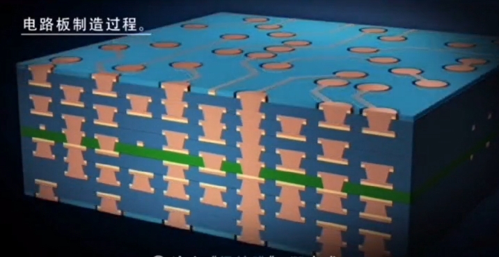
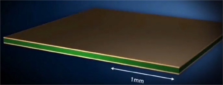
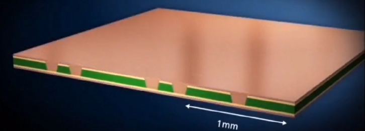
Circuit boards are mainly composed of “copper” and “resin”.


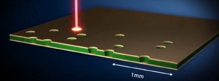
1. Pre-treatment of the copper surface using laser processing.

2. Using “laser processing” drill holes with “a diameter of approximately 0.1mm” in the copper foil and resin.

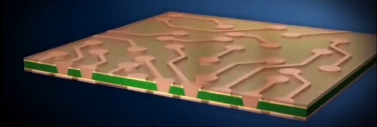
3. Plating with copper, followed by filling the holes.

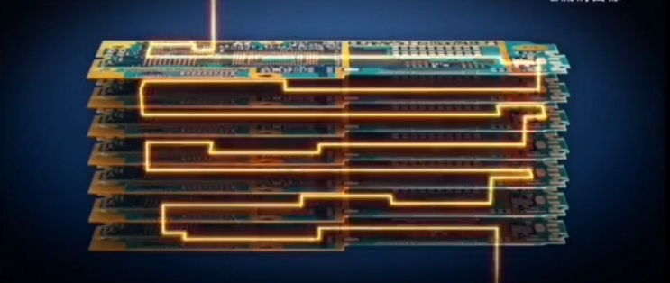
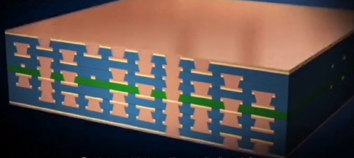
4. Through “chemical treatment”, the copper foil forms the “Continuous circuit” .

Request PCB Manufacturing & Assembly Quote Now

5. Resin and copper foil are pressed together on both sides.

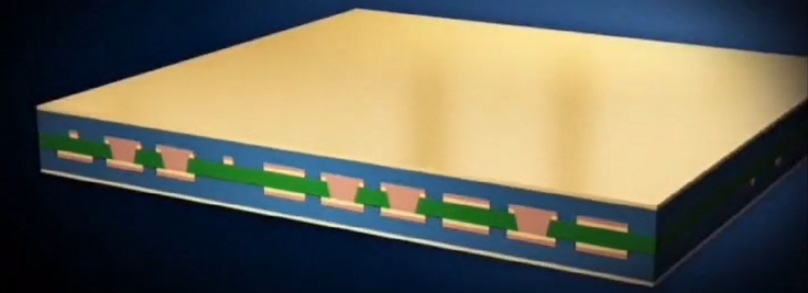
6. The same process is repeated to form the circuit.

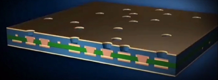
7. “A protective film” is applied, completing the process.


Request PCB Manufacturing & Assembly Quote Now

The resulting circuit board, by conducting electricity through the copper circuit, connects electronic components, performing the function of wiring and enabling all possibilities in all fields.


Related News

SMT patch process and precautions

SMT patch process and precautions

Why PCBA boards get deformed?

Why PCBA boards get deformed?

How to choose the right stacking scheme when designing PCBs

How to choose the right stacking scheme when designing PCBs

SMT solder process - solder paste printing

SMT solder process - solder paste printing

SMT Process Flow Introduction

SMT Process Flow Introduction

High-speed PCB general layout, circuit principles

High-speed PCB general layout, circuit principles

Product Categories

  • PCBA
  • Rigid PCB
  • HDI PCB
  • Rigid Flex PCB
  • Flex PCB
  • High Frequency PCB
    • Rogers PCB
    • Isola PCB
    • Arlon PCB
    • Nelco PCB
    • Taconic PCB
    • Teflon PCB
    • Neltec PCB
  • Metal Core PCB
    • Aluminium PCB
    • Copper PCB
  • Ceramic PCB
  • Laser Stencil
  • Reverse engineering
  • Purchasing components

Links

Google.comBaidu.com

内页左侧广告1

Feedback

Contact Us

sales@key-pcba.com

234123644@qq.com

Commercial and Cultural Building, Community 11 of Tangwei,Fuhai Street, Bao'An District Shenzhen 518103 GuangDong China.

WECHAT

Copyright © 2016 KEY TECHNOLOGY(HK)CO. ,LIMITED All Rights Reserved.

  • Skype.
  • E-mail
  • Whatsapp
  • Inquiry