
Information sharing RF PCB layout and circuit optimization
[Read more] 2-layer PCB manufacturing costs will be lower than 4-layer PCB, but PCB thickness should not exceed 0.8mm - 1.00mm, and the transmission line does not have enough reference distance, the width will become quite large. Like many Rogers RF PCB boards are very thin, generally divided into cavity design, not suitable for large sizes. 4-layer PCB is usually 1.6mm thick, if not on the surface to go RF Signal, can be in the middle layer to go RF line, characteristic impedance of 50Ω.General RF single-chip transceiver program PCB Layout when the double-layer board and 4-layer board layout is predominant, today to see what specific differences.
Cost - the same size, 2-layer board is cheaper
2. PCB thickness
2-layer PCB manufacturing costs will be lower than 4-layer PCB, but PCB thickness should not exceed 0.8mm - 1.00mm, while the transmission line does not have sufficient reference distance, the width will become quite large. Like many Rogers RF PCB boards are very thin, generally divided into cavity design, not suitable for large sizes. 4-layer PCB is usually 1.6mm thick, if you do not go RF Signal on the surface, you can go RF lines in the middle layer, the characteristic impedance is 50Ω.
3. EMI
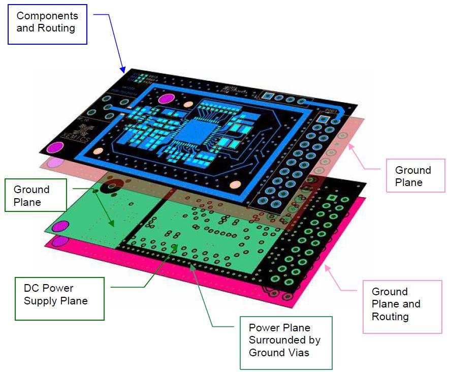
4-layer board as shown above, from the top down are Signal, GND, POWER, GND 4-layer board, placed between the 2 GND a power layer can be between the power and ground to achieve a uniform distribution of RF decoupling capacitance and low impedance at high frequencies. power Plane surrounded by vias, thus preventing any radiation emitted from the edge of the board. As can be seen from the diagram above, the power plane is suppressed at the final stage of the TX matching network to prevent any parasitic coupling caused by radiated and reflected energy at this stage (this part is particularly important to note, as the signal is strongest when transmitting and peripheral signals tend to couple the transmit signal and thus create parasitic modulation).
In contrast, the 2-layer board does not have enough space for a separate power supply layer and full GND, the radiated emission signal cannot be effectively suppressed and EMI is relatively poor.
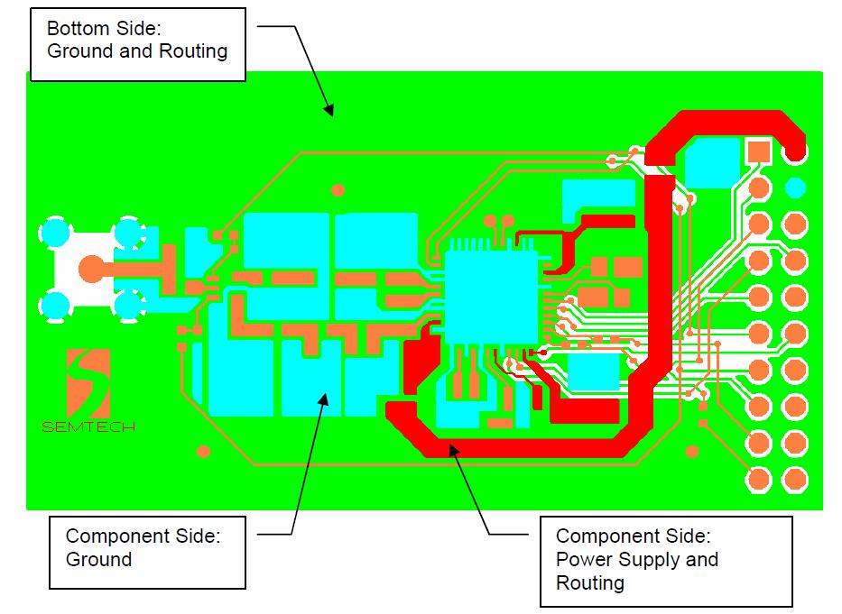
As shown in the diagram above, the power supply routing on the component is very thick in order to present as low an impedance as possible. The large ground area on this side of the board provides a low decoupling impedance path. Wherever possible, try to have a full GND plane underneath.
4. FCC Certification
Every electronic device sold or manufactured in the USA must be officially approved by the Federal Communications Commission (FCC). 4-layer boards have relatively good EMI and are more likely to pass the Part 15 test for intentional/unintentional radiation from electronic products or devices.


