
How to determine the number of PCB layers?Introduction to the PCB board reverse engineering process!
[Read More] To improve your knowledge and understanding of the PCB, this article will be the process and skills of PCB board dissection, as well as the method of determining the number of layers of PCB board to be introduced.The use of PCBs is very widespread, it can be said that the electronic equipment inside the PCB circuit board. To improve your knowledge and understanding of PCB, this article will be introduced to the process of PCB board reverse engineering and skills, as well as the method of determining the number of layers of PCB board. If you have an interest in PCB, and I may wish to continue to read carefully down Oh.
First, the process of PCB board reverse engineering and skills
PCB board reverse engineering is an important element of PCB design. But because it involves sandpaper grinding board (a harmful type of work), tracing (a simple repetitive labor), many designers do not want to engage in this work. Even many designers believe that PCB board reversing engineering is not technical work, junior designers can be competent in this work with a little training. This concept has a certain degree of universality, but as with many jobs, there are still some skills in PCB board reversing. If designers master these skills can save a lot of time, but also can significantly reduce the amount of labour. Here we will talk about this aspect of knowledge in detail.
a, the concept of PCB board reverse engineering
PCB board reverse engineering is the process of getting the schematic and board diagram (PCB diagram) based on the original PCB board physical. Its purpose is to carry out later development. Post development includes installation of components, deep testing, modification of circuits, etc. Because it does not belong to the scope of PCB board reversing and related, so only to introduce not to elaborate.
b, the process of PCB board disassembly
1, remove the original board on the device.
2, the original board will be scanned to get the graphics file.
3, the surface layer will be ground away to get the intermediate layer.
4, the intermediate layer will be scanned, get the graphics file.
5、Repeat steps 2-4 until all layers have been processed.
6, using special software to convert the graphics file into an electrical relationship file - PCB diagram. If the right software is available, the designer can simply trace the graphics over.
7, check and verify to complete the design.
c, PCB board reversing skills
PCB board reverse engineering, especially multi-layer PCB board reversing is a time-consuming and laborious work, which includes a lot of repetitive work. Designers must have enough patience and care, otherwise it is very easy to produce errors. The key to good reverse-out PCB design is to use the right software instead of manual repetitive work, that is, to save time and accuracy.
1, choose the best conversion software
The conversion of the scanned graphics file into a PCB file is the key to the whole job. With a good conversion file. Designers only need to "copy the cat", the graphics will be traced once to complete the work. EDA2000 is recommended here, it is really convenient.
2, the process of reverse engineering must be used in the scanner
Many designers are used to directly in PROTEL, PADSOR or CAD and other PCB design systems on the drawing line. This habit is very bad. Scanned graphic files are both converted into PCB files on the basis of, and later to check the basis. Using a scanner can greatly reduce the difficulty and intensity of labour. It is no exaggeration to say that if you can make full use of the scanner, even if no design experience personnel can also complete the work of PCB board reverse engineering.
3, unidirectional grinding board
Some designers in pursuit of speed, choose two-way grinding board (i.e., from the front and rear surface to the middle layer of grinding off the board layer). In fact, this is very wrong. The outer layer of the PCB board is the hardest due to the process and the presence of copper foil, pads and other reasons, and the middle layer is the softest. Therefore to the middle layer, the problem is more serious, often unable to polish. In addition, various manufacturers produce PCB board material, hardness, flexibility are not the same, it is difficult to accurately grind away.
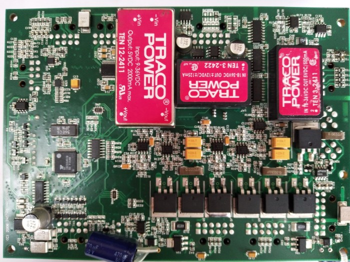
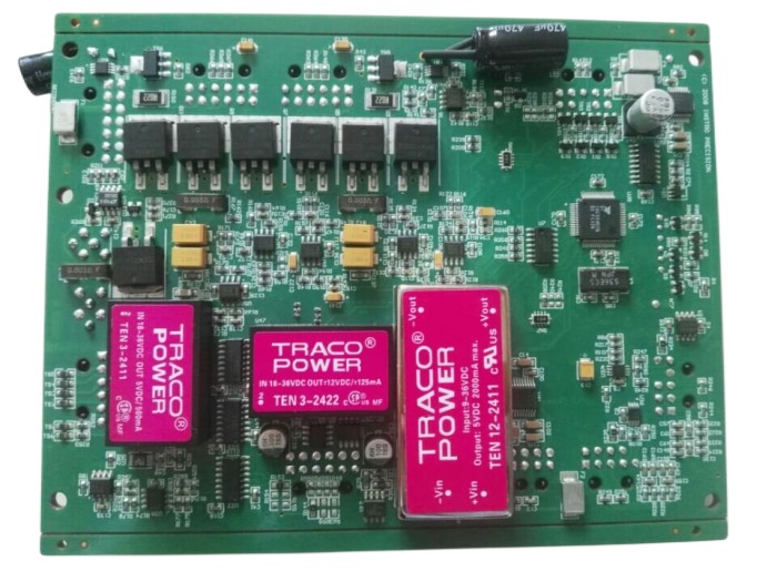
Second, the number of PCB board layers to judge
Single-sided PCB: is only one side of the PCB board has lines (can have holes, can also be no holes), the other side of the substrate or direct insulation ink cover, without any lines and placed under strong light the whole board translucent (excluding individual plates and process special requirements). The cross-section contains copper foil only on the side with lines.
Double-sided PCBs: the common PCB with lines on both sides, with copper holes as a "bridge" linking the two sides of the board and with the whole board translucent under bright light (excluding individual boards and special process requirements). Only the outermost two sides of the PCB contain copper foil in the cross-section.
Multi-layer PCB: On the basis of a double-sided board like a "sandwich" with a sandwich PCB in the middle (depending on manufacturing capacity, generally 4 to 12 layers for mobile phones, computers, home appliances, cars. Military or aerospace, positioning, 8 to 20 layers. Satellite, navigation, rocket, etc. can reach more than 60 layers, its precision can be imagined. In fact, the CPU can also be understood as an ultra-precise "PCB" in microelectronics). The middle layer is generally called the "inner layer". Multilayer PCBs are opaque or partially opaque and inconspicuous in bright light, with the outermost two ends of the cross-section and the middle position containing copper foil.
In the case of single-sided, double-sided and multilayer PCBs with the same board and volume, the weight of the multilayer PCB is "the weight of the double-sided PCB" and "the weight of the single-sided PCB.


 HDI PCB PROCESS")
