
Can PCB vias on the PAD?
In PCB design, whether the vias can be punched on the pads or not needs to be decided according to the specific application scenarios and design requirements.
If it's in a personal DIY situation, punching the over holes into the pads probably won't create too much of a problem.
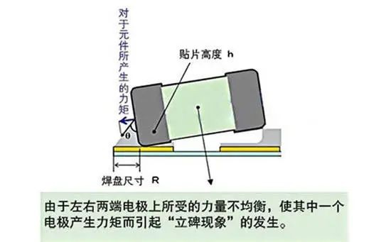
However, in the case of SMT placement production, this can lead to the phenomenon of "standing monuments". This is because the surface tension of the solder will pull the components to stand up, leading to problems such as false soldering, desoldering and poor contact. Especially for small packaged components, such as chip capacitors and chip resistors, the stand-up phenomenon is more likely to occur. To prevent this, it is sometimes necessary to do windowing on copper-laying pins.
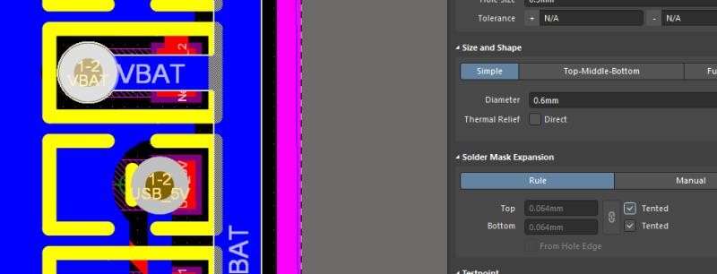
In addition, if the plugging of the over-hole is not done properly, it may lead to tin leakage, which further triggers the phenomenon of standing monument. Therefore, the location of the vias also needs to be considered in the process.
Therefore, in order to ensure the reliability of the PCB design and the smooth progress of the process, the over-hole try not to hit directly on the pad. However, the following situation, the over-hole in the pad, the problem is not too big, it is OK.
Situation 1:
If the perforations are punched on the back of large pads, for example, in order to improve the heat dissipation of MOSFETs and perforated on the pads of MOSFETs, this is OK. It should be noted that the perforation treatment of large pads needs to be evenly distributed to ensure that the pads are evenly heated.
Situation 2:
If you need to punch over holes in hot pads, for example, in order to heat dissipation for IC heat dissipation over holes, due to the chip body in the middle of the chip body does not need to be soldered pins, so the over holes in the IC heat dissipation pads do not need to take into account the tin leakage, false soldering and other issues.
In summary, whether or not you can punch holes in the pad, you need to evaluate and make decisions based on specific design requirements and process conditions. At the same time, it is also necessary to consider the location, size, number of perforations and other parameters to meet the circuit performance and reliability requirements. In practice, it is recommended to consult a professional PCB design engineer or PCB manufacturer for accurate advice and guidance.
Related News


