Why can't I hit the via hole on the pad? I just want to punch, what should I do?
Why can not hit the via hole on the pad, I would like to hit, how?Many newcomers to the PCB often have this problem when they first come into contact with the board space is too small, the device is dense, resulting in a small space, can not lead to fan holes, usually choose to punch the hole in the pad, which makes it much easier to connect their own, but often unclear what kind of problems will lead to the board? Can you play this way?
In order to make this problem clearer explanation, will be elaborated from the following two aspects, respectively:
1) Why can't the over-hole be punched on the pad?
2) What can be punched on the pads under what circumstances?
1, why can not hit the hole in the pad?
Earlier in the PCB design is not allowed to have holes in the BGA pads, the main reason for fear of tin leakage leads to insufficient solder paste on the pads, which leads to device soldering when the device is false, desoldering, so the general device on the hole are first lead out and then punch holes.
At this stage, due to the shrinking pitch of the BGA, through the resin plug hole, there will be no more tin leakage, but the hole in the pad, there is a risk of false solder or off, the cost will increase, will also affect the PCB board aesthetics, so it is generally not recommended to do so.
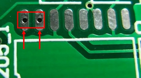
The phenomenon of "standing monument" often occurs in the reflow soldering process of CHIP components (such as chip capacitors and chip resistors), the smaller the component volume, the more likely to occur, for example, 0201, 0402 and other small chip components. In the reflow soldering process of surface mount process, the SMD components produce the phenomenon as shown in the figure, because a section of the components warped lead to desoldering, because of this situation, generally image called "standing stone" phenomenon.
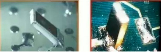
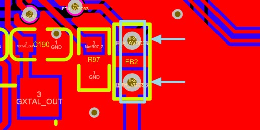
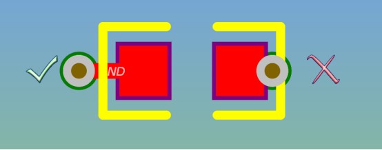
The "monolith" phenomenon is due to the component pads on both ends of the solder paste in the reflow melting, the component two solder end of the surface tension imbalance, the tension of the larger end pulling the component along its bottom rotation and caused. Some small packages of chip resistors and capacitors, it is best not to hit the hole in the pad for the same reason, the hole in the edge of the pad, due to the tension at both ends of the pad is not consistent and easy to produce the phenomenon of standing monument.
2, under what circumstances can the hole in the pad?
(1) buried blind hole
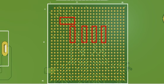
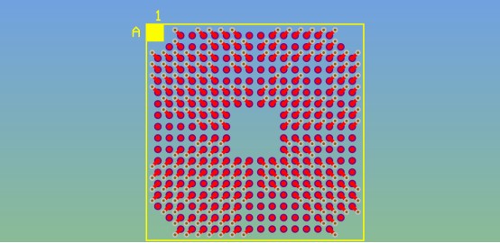
Generally speaking, when the BGA pitch is less than or equal to 0.5mm state, the BGA is not good at this time to fan out the hole, in this case, you can take the blind buried hole to solve the way.
Blind vias (Blind vias ): Blind vias are the PCB inner alignment and PCB surface alignment connected to the type of hole, the hole does not penetrate the entire board. For example, only from the surface layer to the middle of the third layer.

Buried vias (Buried vias): Buried vias are the type of vias that connect only the inner layers of the alignment, so it is not visible from the surface of the PCB.


As the blind hole only through the surface to the inner layer, not all through the PCB, so it does not lead to tin leakage, and buried holes directly from the internal hole, so there is no such concern, the only problem is still from the cost to consider, buried blind hole process manufacturing costs will be greatly increased.
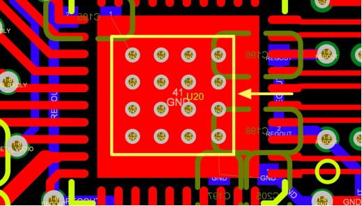
(2) thermal over-hole
In the PCB design often see the design shown below, commonly found in the recommended design of the chip, requiring the thermal pads on the hole, this case is for the IC heat dissipation and heat dissipation hole. As the chip body does not need to be soldered in the middle of the pin, so the hole in the IC thermal pad is not to consider the leakage of tin, false solder and other issues.