
The difference between blind buried hole circuit board and HDI board
The difference between blind buried hole circuit board and HDI board
HDI belongs to a product of the circuit board, the full name is high Density Interconnection, high-density interconnection board at present, high-grade electronic products are generally HDI board products.Blind vias are the PCB inner alignment and PCB surface alignment connected to the type of over-hole, the hole does not penetrate the entire board.
Buried holes are only connected between the inner layer of the alignment of the hole type, so it is not visible from the surface of the PCB.
With the current design of portable products toward the direction of miniaturization and high density, PCB design is becoming increasingly difficult, the PCB production process to put forward higher requirements. In most of the current portable products so that the 0.65mm pitch below the BGA package, are using a blind buried hole design process, then what is a blind buried hole?
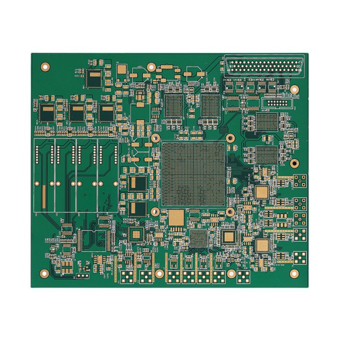
HDI circuit board
Blind vias are the PCB inner alignment and circuit board surface alignment connected to the type of over-hole, the hole does not penetrate the entire board.Buried holes are only connected between the inner layer of the alignment of the type of hole, so it is not visible from the surface of the PCB.
Buried blind holes in the board is not necessarily HDI circuit board, but the general HDI board have blind holes, buried holes are not necessarily, depending on your board products are a few orders of several pressure products.
Description as follows.
6-layer circuit board 1step, 2step is for the need for laser drilling of the board, that is, refers to the HDI board.6-layer circuit board 1step HDI board refers to the blind hole: 1-2, 2-5, 5-6. That is, 1-2, 5-6 need laser drilling.
6-layer circuit board 2step HDI board refers to blind holes: 1-2,2-3,3-4,4-5,5-6. that is, 2 laser drill is required.
First drill 3-4 buried holes, then press fit 2-5, then drill 2-3, 4-5 laser holes for the first time, then press fit 1-6 for the second time, then drill 1-2, 5-6 laser holes for the second time. Finally, the through-hole is drilled. This shows that the 2step HDI board has been stack-up together twice and laser drilled twice.
In addition, 2step HDI plates are also divided into: different position-hole 2step HDI plates and stacked-hole 2step HDI plates, different position hole 2ND HDI plates means that blind holes 1-2 and 2-3 are staggered, while stacked-hole 2step HDI plates means that blind holes 1-2 and 2-3 are stacked together, for example: blind: 1-3, 3-4, 4-6.
And so on 3step, 4step...... are the same.


