
How to control the cost of PCB assembly?PCB board reverse tips for free!
[Read More] To improve your knowledge of PCB boards, this article will introduce the skills of PCB board dissection and how to control the cost of PCB board assembly.
PCB board is one of the most commonly used electronic devices, almost all electronic devices have a PCB board figure. To improve your knowledge of PCBs, this article will introduce the skills of PCB board reverse and how to control the cost of PCB board assembly. If you are interested in PCBs, you may wish to read on with the editor.
First, the skills of PCB board reverse
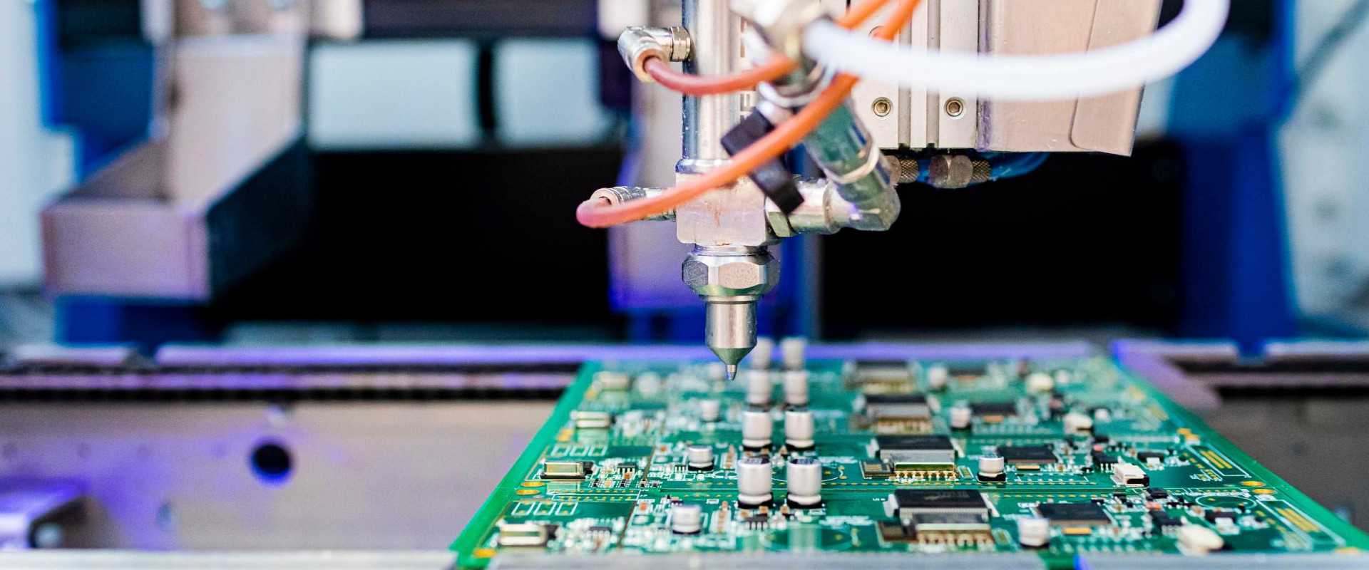
PCB board reverse, especially multi-layer PCB board reverse is a time-consuming and laborious work, which contains a lot of repetitive work. Designers must have enough patience and care, otherwise it is very easy to produce errors. The key to good reverse-out PCB design is to use the right software instead of manual repetitive work, that is, to save time and accuracy.
1, choose the best conversion software
The conversion of the scanned graphics file into a PCB file is the key to the whole job. With a good conversion file. Designers only need to "copy the cat", the graphics will be traced once to complete the work. EDA2000 is recommended here, it is really convenient.
2, the process of profiling must be used in the scanner
Many designers are used to directly in PROTEL, PADSOR or CAD and other PCB design systems on the drawing line. This habit is very bad. Scanned graphic files are converted into PCB files on the basis of both, but also later to check the basis. Using a scanner can greatly reduce the difficulty and intensity of labour. It is no exaggeration to say that if you can make full use of the scanner, even if no design experience personnel can also complete the PCB board profiling work.
3, unidirectional grinding board
Some designers in pursuit of speed, choose two-way grinding board (i.e., from the front and rear surface to the middle layer of grinding off the board layer). In fact, this is very wrong. The outer layer of the PCB board is the hardest due to the process and the presence of copper foil, pads and other reasons, and the middle layer is the softest. Therefore to the middle layer, the problem is more serious, often unable to polish. In addition, various manufacturers produce PCB board material, hardness, flexibility are not the same, it is difficult to accurately grind away.
Second, how to control the cost of PCB assembly
PCB assembly costs, every electronic engineer or designer wants to know how to get the best quote for PCB assembly, and how price affects PCB assembly costs. Here are some tips to guide you on how to control the price of PCB assembly.
First, clearly understand the attributes of PCB assembly (PCBA) costs. Some of the biggest cost drivers include:
(1) Assembly type Surface Mount (SMT) (SMD element) Through Hole (DIP) Mixing (both)
(2) Component placement requests only the top-level component requests Doulbe two-sided assembly
(3) Total number of components (SMD+DIP)
(4) Component package size 1206 0804 0603 0402 020101005
(5) Component packaging (reel priority) reel pipe tray with or without tie reverse strip loose packaging bag
(6) Required process SMT patch through-hole automatic insertion through-hole sliding line wave soldering automatic optical inspection (AOI)
X-ray selective solder manual solder assembly
(7) Quantity and batch size
"Keep Panelize flexible to meet your manufacturer's needs."
You need to ensure that the panelization has been optimized for the needs of PCBA manufacturers.
(8) Special part preparation requirements (i.e. lead length, minimum/maximum height, spacing)
(9) Total cost of complete bill of materials (BOM)
(10) Number of bare board (PCB) layers and materials used
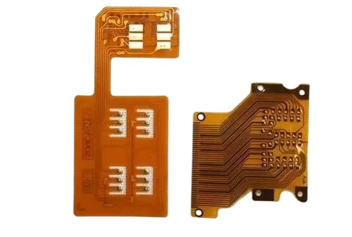
The cost of flexible PCB assembly is higher than that of rigid PCB
(11) Coating requirements (full coating or selective coating is usually required for medical or military purposes) Coating quantity sprayed or brushed - coating area specified by coating tolerance
(12) Potting requirements (if any)
(13) Assembly compliance requirements RoHS (lead-free) non-RoHS (lead-containing) IPC-A-610D Class I, II or III ITAR
(14) Test requirements (KEY prefers to test all PCBA boards before shipment, and we hope you can tell us how to test) Power-on function circuit test (ICT) No test for cycling (only visual inspection)
(15) Transportation requirements Standard ESD (electrostatic discharge) bag non-standard/special container
(16) Delivery (KEY provides fast rotation pcb assembly service)
Standard shift, no urgent requirement for rapid conversion (labor and material costs are affected)
These 16 tips will affect the price of pcb assembly, so you can choose the best one to save costs. When you purchase parts, you can provide multiple component sources for each component, which is easy to control some costs. Not only from digikey, but also some agents have a powerful price to support a component, which can reduce the cost sources more quickly
Set up the process to obtain low-cost resources between your design engineering and procurement departments. This is easier said than done. Conflicts of priorities between design engineering and procurement may hinder this process.
One solution is to establish a material cost reduction committee. Management works with Procurement and Engineering to identify high value cost reduction opportunities. They are also committed to identifying strategic components that require multiple sources to ensure continuous production.


