PCB impedance calculation
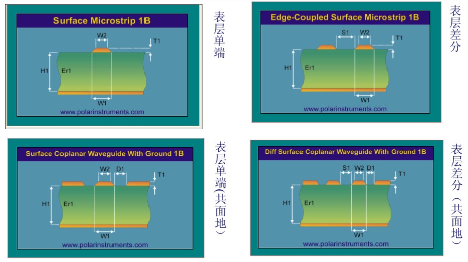
I: Common patterns in usual impedance calculations1:Surface impedance
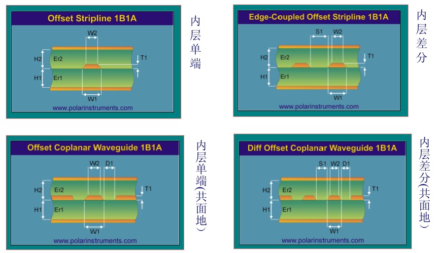
2: Inner layer impedance
II: the conditions required in the design
Board Thickness
Number of layers, number of signal layers, number of power layers
Substrate material
Surface technology
Impedance value
Impedance Tolerance
Copper Thickness
Inspection standard
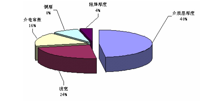
2, from the PCB production point of view, the impact of impedance resistance value has 7 key factors, dielectric thickness (H), dielectric constant (DK), copper thickness (T), copper residual rate, line width (W), line spacing (S), soldermask thickness.
a Dielectric thickness H
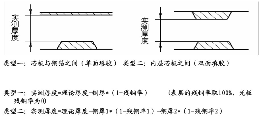
Such as the following diagram in the value of H that is the thickness of the medium, the thickness of the medium is the most important factor affecting the impedance value, the impedance can be controlled to see this point. The thickness of the medium is proportional to the resistance value, increase the thickness of the medium can improve the impedance value, and vice versa to reduce the thickness of the medium can reduce the impedance value of the different PP (bonding sheet) has a different glue content and thickness, the actual thickness of its compression is not the same, so it is necessary to match the thickness of H according to the calculated.
b Dielectric constant (DK)
Dielectric constant is inversely proportional to the impedance, increase the dielectric constant can reduce the impedance, reduce the dielectric constant can increase the impedance, dielectric constant is mainly through the material material to control. The dielectric constant of different materials are different, and the material used, such as FR4 material, its dielectric constant is about 3.8-4.8 between the dielectric constant of this material is unstable is not suitable for use in high-frequency circuits. PTFE material has a dielectric constant of 2.2-3.9, which is much more stable than FR4, so it is commonly used in high-frequency boards.
c Copper thickness (T)
Copper thickness and impedance is inversely proportional to the increase in copper thickness can reduce the impedance, and vice versa, reduce the copper thickness can increase the impedance, copper thickness can be controlled through the graphic plating or selection of the corresponding thickness of the base material copper foil. The control of copper thickness requires uniformity, for fine lines, isolated lines need to be compensated for more, or split on the shunt copper block, so that the current balance, to prevent uneven thickness of copper on the line to affect the impedance.
d trace width and spacing (W,S,D)
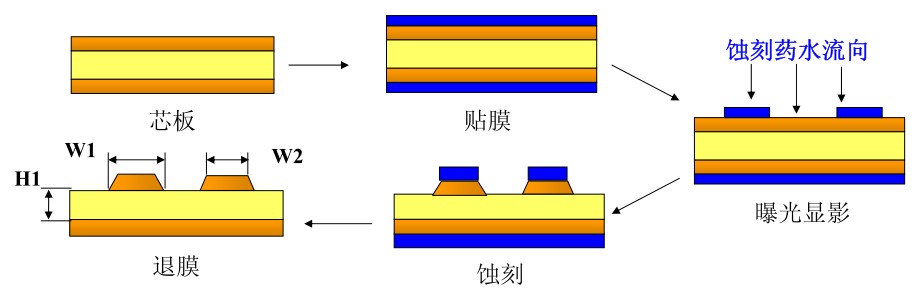
trace width is inversely proportional to impedance, increase trace width can reduce impedance, reduce trace width can increase impedance, trace spacing is proportional to impedance, increase trace width can increase impedance, reduce trace width can reduce impedance. trace width tolerance is generally controlled by +/-10%, the signal trace has a gap will affect the entire test waveform, so the impedance trace is not allowed to have a complementary trace, there are gaps in the situation, trace width and trace spacing accuracy is mainly controlled by etching, in order to ensure that the trace width and trace spacing, the process will be based on the etching side of the etching amount of error code difference in the light drawing, trace graphic transfer error, the engineering film for the special process of compensation in order to achieve the required trace width and trace spacing.
e Soldermask Thickness
Printing on the solder resist will make the outer layer impedance decrease, the thickness of the solder resist is inversely proportional to the impedance, under normal circumstances, printing a single solder resist can make the single-ended impedance down 2 ohm, can make the differential impedance down 5-6 ohm, printing two solder resist can be reduced by two times. All the boards with impedance should be clearly labelled as to the thickness of the soldermask and whether the impedance line is covered with soldermask oil or not.
III: impedance calculation
Impedance calculation Audemars Piguet circuit mainly used in the calculation software for Polar-SI9000, this software contains a total of 93 impedance calculation mode, commonly used for the article mentioned in the beginning of the 8 kinds. The calculation process will generally be based on the requirements or documents whether to use the cover soldering calculation or not cover soldering calculation.

Impedance Calculation Method
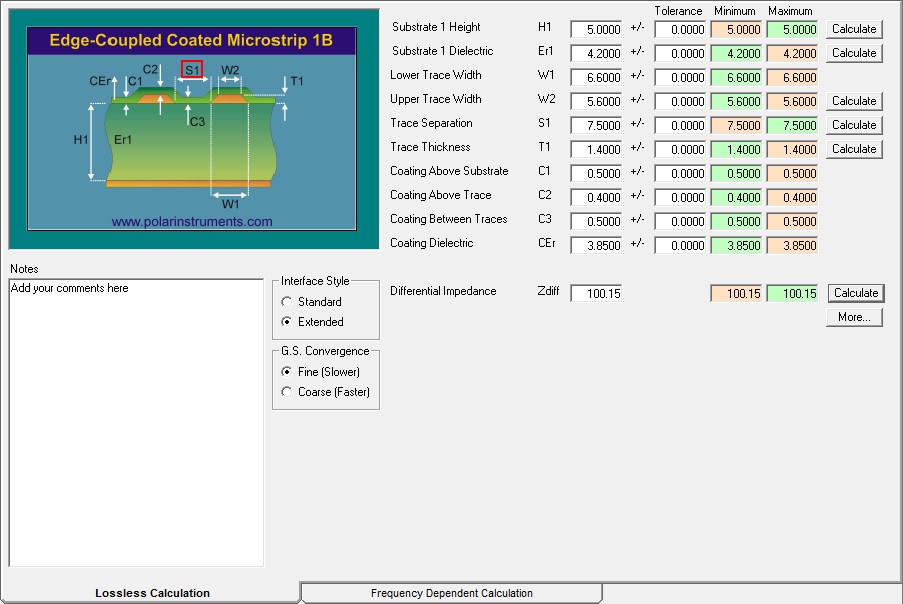
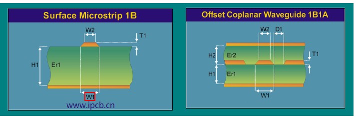
Outer layer differential impedance cover soldermask calculation
H1 Dielectric thickness
Er1 Dielectric constant of dielectric degree
W1 Line width
W2 Upper line width
S Spacing
T Copper thickness
C Soldermask thickness
Er2 Resistance dielectric constant
The reason for the difference between W1 and W2 is shown in the following diagram. Due to the production of etching solution on the surface of the copper contact is sufficient, and the contact with the following is relatively small, so the etching out of the line width under a magnifying glass to see the shape of the trapezoid, and W1 is greater than W2, so there is a division of W1 and W2 that is what we call on the upper line width, the lower line width of the difference between the general for the 0.5-1 mil, which will be able to get a more accurate value of the impedance.
Copper thickness 0.5oz(17um),1oz(35um),2oz(70um)
Commonly used PP (bonding sheet) specifications and corresponding thickness:
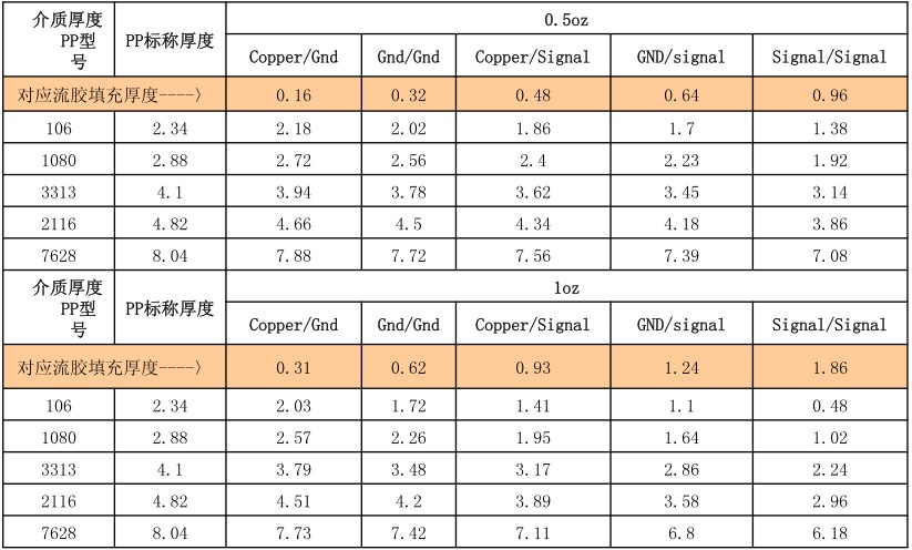
The method of calculating the actual thickness of the adhesive sheet after taking into account the flow of glue and filler for the parameters involved in the impedance calculation.