KEY TECHNOLOGY(HK)CO. ,LIMITED
  • Home
  • Products
    • PCBA
    • Rigid PCB
    • HDI PCB
    • Rigid Flex PCB
    • Flex PCB
    • High Frequency PCB
      • Rogers PCB
      • Isola PCB
      • Arlon PCB
      • Nelco PCB
      • Taconic PCB
      • Teflon PCB
      • Neltec PCB
    • Metal Core PCB
      • Aluminium PCB
      • Copper PCB
    • Ceramic PCB
    • Laser Stencil
    • Reverse engineering
    • Purchasing components
  • Capability
    • PCBA capability
    • Rigid PCB capability
    • HDI PCB Capability
    • Rigid Flex PCB Capability
    • Flex PCB Capability
    • High Frequency PCB Capability
    • Metal Core PCB Capability
    • Ceramic PCB Capability
  • Equipment
    • PCB Equipment
    • PCBA Equipment
  • About us
  • Blogs
  • Feedback
  • Contact us

Blogs

  1. Home
  2. Blogs
  3. RK3588 VDD CPU LIT Power Supply PCB Desi...

RK3588 VDD CPU LIT Power Supply PCB Design

RK3588 VDD_CPU_LIT Power PCB Design


1, VDD_CPU_LIT copper cladding width to meet the chip current requirements, connected to the chip power supply pins of the copper cladding is wide enough, the path can not be divided by the over-hole is too serious, you must calculate the effective width of the line, to confirm that the path connected to the CPU each power supply PIN pin are enough.

2, VDD_CPU_LIT power supply in the peripheral layer, as much as possible to play the power supply over-hole (more than 9 0.5 * 0.3mm over-hole), to reduce the voltage drop brought about by the layer over-hole; decoupling capacitor GND over-hole with its power supply over-hole to maintain the same number of holes, otherwise it will greatly reduce the role of capacitance.

3, as shown in Figure 1, the schematic near the RK3588 VDD_CPU_LIT power supply pin green line within the decoupling capacitors must be placed on the back of the corresponding power supply pin, capacitor GND PAD as close as possible to the chip centre of the GND pin placed, as shown in Figure 2. The rest of the decoupling capacitors are placed as close as possible to the RK3588 chip, and need to be placed in the path of the power split source.

4, RK3588 chip VDD_CPU_LIT power supply pins, each pin near a corresponding hole, and the top walk "well", cross-connections, as shown in Figure 3, it is recommended that the alignment of the line width of 10mil.


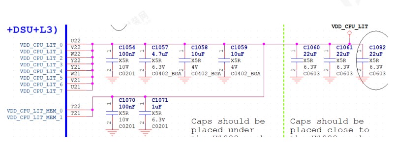
Figure 1 VDD_CPU_LIT schematic power supply pin decoupling capacitor


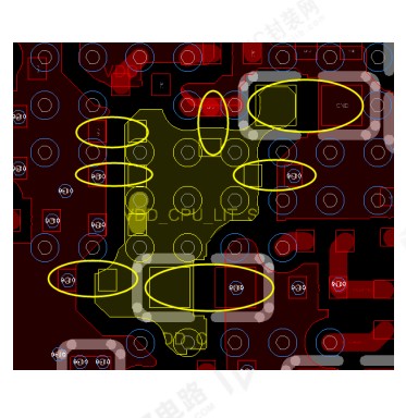
Figure 2 Decoupling capacitor placement on the back of the power supply pin


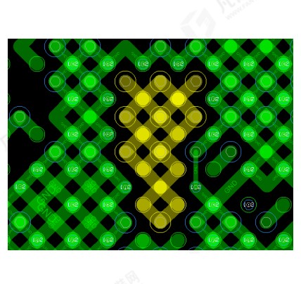
Figure 3 VDD_CPU_LIT power supply pin "well" chain

5, VDD_CPU_LIT power supply in the CPU area line width shall not be less than 120mil, the peripheral area width of not less than 300mil, the use of dual-layer power copper cladding to reduce the alignment of the voltage drop (other signals for the layer of holes, please do not arbitrarily placed, must be placed in a regular rule, as far as possible to make room to go to the power supply, but also conducive to the ground layer of copper cladding, as shown in Figure 4).


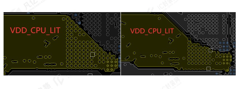
Figure 4 VDD_CPU_LIT power layer copper cladding situation

6, power over the hole 40mil range (over the hole centre to over the hole centre spacing) within the number of GND over the hole, it is recommended that ≧ 9. As shown in Figure 5.


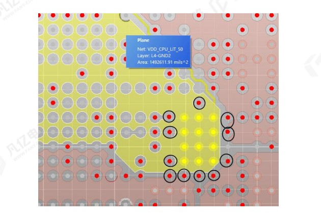
Figure 5 LIT power ground over-hole placement map

Related News

What is ICT?

What is ICT?

Skills of manual soldering of chip electronic components

Skills of manual soldering of chip electronic components

How much does multi-layer PCB manufacturing cost?

How much does multi-layer PCB manufacturing cost?

The function and design requirements of PCBA board splitter

The function and design requirements of PCBA board splitter

FR-4 sheet process

FR-4 sheet process

How to optimise switching power supply layouts by minimising thermal circuit PCB ESR and ESL?

How to optimise switching power supply layouts by minimising

Product Categories

  • PCBA
  • Rigid PCB
  • HDI PCB
  • Rigid Flex PCB
  • Flex PCB
  • High Frequency PCB
    • Rogers PCB
    • Isola PCB
    • Arlon PCB
    • Nelco PCB
    • Taconic PCB
    • Teflon PCB
    • Neltec PCB
  • Metal Core PCB
    • Aluminium PCB
    • Copper PCB
  • Ceramic PCB
  • Laser Stencil
  • Reverse engineering
  • Purchasing components

Links

Google.comBaidu.com

内页左侧广告1

Feedback

Contact Us

sales@key-pcba.com

234123644@qq.com

Commercial and Cultural Building, Community 11 of Tangwei,Fuhai Street, Bao'An District Shenzhen 518103 GuangDong China.

WECHAT

Copyright © 2016 KEY TECHNOLOGY(HK)CO. ,LIMITED All Rights Reserved.

  • Skype.
  • E-mail
  • Whatsapp
  • Inquiry