KEY TECHNOLOGY(HK)CO. ,LIMITED
  • Home
  • Products
    • PCBA
    • Rigid PCB
    • HDI PCB
    • Rigid Flex PCB
    • Flex PCB
    • High Frequency PCB
      • Rogers PCB
      • Isola PCB
      • Arlon PCB
      • Nelco PCB
      • Taconic PCB
      • Teflon PCB
      • Neltec PCB
    • Metal Core PCB
      • Aluminium PCB
      • Copper PCB
    • Ceramic PCB
    • Laser Stencil
    • Reverse engineering
    • Purchasing components
  • Capability
    • PCBA capability
    • Rigid PCB capability
    • HDI PCB Capability
    • Rigid Flex PCB Capability
    • Flex PCB Capability
    • High Frequency PCB Capability
    • Metal Core PCB Capability
    • Ceramic PCB Capability
  • Equipment
    • PCB Equipment
    • PCBA Equipment
  • About us
  • Blogs
  • Feedback
  • Contact us

Blogs

  1. Home
  2. Blogs
  3. What is PCBA gold finger get soldering?...

What is PCBA gold finger get soldering?

In the smt placement process, you may encounter the phenomenon of gold finger staining, that is to say, in the printing/soldering process pcb board yellow conductive contacts stained with solder paste, thus affecting the performance of the product.


First, why the phenomenon of tin staining
1, the printing machine pressure is too large, resulting in part of the solder paste is squeezed out of the control range;
2, excessive pressure of the mounter;
3, reflow soldering preheating time is short, the heating speed is fast;
4, stencil design, the opening size is unreasonable;
5, there is pollution of equipment;

Second, how to avoid the phenomenon of tin staining

1, in terms of process:
1)adjust the appropriate squeegee pressure, wipe frequency and the spacing between the printing plate and stencil.
2)Appropriate patch pressure can reduce the tin powder is extruded.
3)Rigorous machine cleaning and maintenance can reduce the pollution index.
4)Reduce stencil opening size.
5)Slow heating rate/higher profile of homogenizing temperature.

2.In terms of materials:
1) Low splatter solder paste helps reduce gold finger tinning.
2) Use solder paste with slow wetting rate.
3) Low moisture parts and PCBs help reduce splatter.
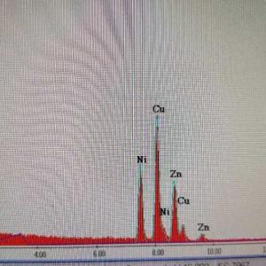
4) Proper gold finger plating reduces exposed nickel.
Tin phenomenon, according to the site environment to analyze, find out the reasons in a timely manner, to be resolved, so as to avoid affecting the quality of PCBA products, reduce the waste of production costs.
Related News

Popular Knowledge, SMD Resistor Marking Interpretation, Read Resistance Value at a Glance

Popular Knowledge, SMD Resistor Marking Interpretation, Read

Electrical clearance and creepage distance details and handling in PCB

Electrical clearance and creepage distance details and handl

PCB design tips and tricks

PCB design tips and tricks

What factors need to be considered for PCB design costs? How can I save on PCB design costs?

What factors need to be considered for PCB design costs? How

SMT patch process and precautions

SMT patch process and precautions

FR-4 PCB Manufacturing process-Drilling

FR-4 PCB Manufacturing process-Drilling

Product Categories

  • PCBA
  • Rigid PCB
  • HDI PCB
  • Rigid Flex PCB
  • Flex PCB
  • High Frequency PCB
    • Rogers PCB
    • Isola PCB
    • Arlon PCB
    • Nelco PCB
    • Taconic PCB
    • Teflon PCB
    • Neltec PCB
  • Metal Core PCB
    • Aluminium PCB
    • Copper PCB
  • Ceramic PCB
  • Laser Stencil
  • Reverse engineering
  • Purchasing components

Links

Google.comBaidu.com

内页左侧广告1

Feedback

Contact Us

sales@key-pcba.com

234123644@qq.com

Commercial and Cultural Building, Community 11 of Tangwei,Fuhai Street, Bao'An District Shenzhen 518103 GuangDong China.

WECHAT

Copyright © 2016 KEY TECHNOLOGY(HK)CO. ,LIMITED All Rights Reserved.

  • Skype.
  • E-mail
  • Whatsapp
  • Inquiry