
How to choose the right stacking scheme when designing PCBs
We all have to draw multilayer PCBs when the layer stack is set, where the more layers of the board stacking scheme, many people do not know enough about multilayer PCBs, usually a good stacking scheme can reduce the interference generated by the board, our stacking structure is an important factor affecting the EMC performance of the PCB board, the following we take four-layer board and six-layer board as an example to introduce their stacking scheme, so that We choose the optimal lamination structure from them.
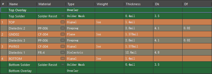
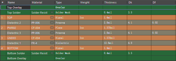
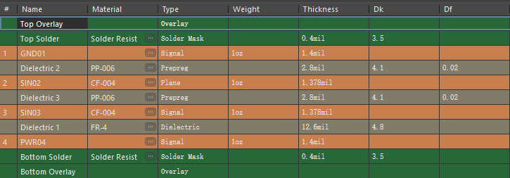
There are three types of lamination structures for four-layer boards, as follows.
The first.
The second.
The third.
We first analyse the first and second lamination, the difference between these two laminations when the second layer and the third layer on the contrary, these two are also four-layer board with more lamination scheme, these two lamination scheme are feasible, just need to be selected according to the actual situation of our board, usually in the four-layer board design we mainly look at the device is mainly placed in the top layer or the bottom layer, our GND layer is mainly Our GND layer is mainly placed close to the device layer, so that it can provide a complete ground plane for the device and thus also shield interference, etc. Our alignment also tries to go in the wiring layer close to the bottom layer, so as to ensure the stability of the signal, but also to avoid cross-sectional situations, which is the difference between these two stacked layer solutions.
Next we look at the third lamination scheme, this lamination scheme is the layer and power distribution in the first and fourth layer, if it is a two-layer board, we need to deal with our signal lines and ground and power in the top and bottom layer, but we are four-layer board, if this lamination is not the advantage of four-layer board, and the signal quality is not very good, two or three layers is the alignment layer, the first thing we need to know is that we The first thing we need to know is that our devices need to be placed in the top and bottom layer, if the top and bottom layer is allocated for ground and power supply, we can not guarantee the integrity of the ground plane, the power supply is also the same, so the second layer of the third layer of the alignment is likely to have no complete reference plane, the interference shielding of this layer stacking scheme is also poor, usually after we draw the board is required to lay the top and bottom layer of the full version of the ground copper skin, this layer stacking scheme to the first layer As a ground layer is really a bit redundant, so this stack for the normal four-layer PCB design will not be selected.
The above is a common stacking scheme for four-layer boards, we can do a selection of the first and second stacking layer according to the actual situation of the board, the following we introduce the common six-layer board stacking.
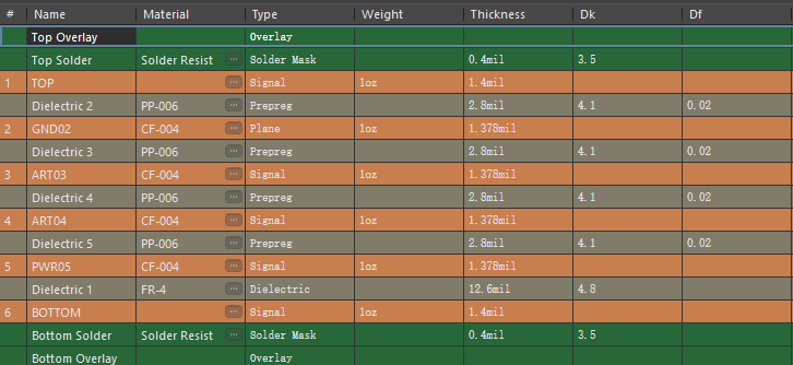
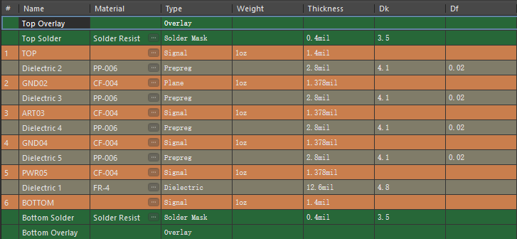
The first kind.
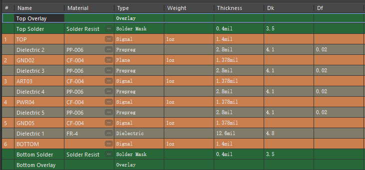
The second kind.
The third.
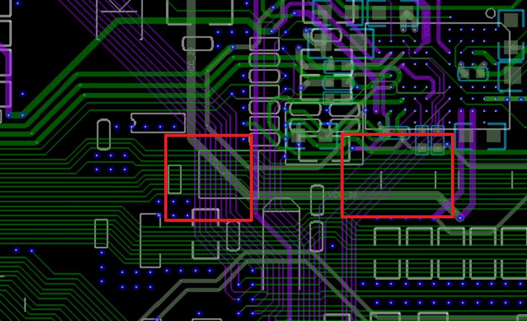
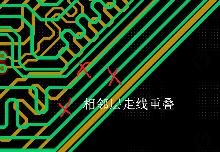
The first lamination scheme has two internal wiring layers to reduce our wiring difficulties, but for the third and fourth layers are adjacent wiring layers, so it is easy to generate crosstalk, so we should pay special attention to adjacent layers when using this lamination scheme to use vertical wiring, to avoid parallel alignment. (As shown in the diagram below).
In the second lamination scheme, the third layer is the signal layer and its adjacent layers are all GND, which can be effectively isolated from other layers and is less prone to crosstalk. There are two internal electrical layers, so that we have asymmetrical internal electrical layers and there is a risk of warping.
The third lamination solution and the second lamination solution compared to the fourth and fifth layers are only swapped, this lamination can also do effective isolation for our signal, but this lamination solution is also the case of the inner electrical layer is not the right layer, so there will also be a warpage situation, this lamination solution, there are two adjacent ground layer, the signal will also be better, in the design time there will be a lot of customer requirements for the need to control This requires the integrity of the reference planes, which are usually relatively intact, and the power planes, which usually require different power signals, and there is a risk of cross splitting if two adjacent planes are referenced.
Through the above introduction we find that each lamination scheme has advantages and disadvantages, we need to select the right lamination according to the actual situation of the board, in the actual design, we found that the first lamination scheme is used particularly high frequency, because for ordinary companies also need to consider the cost, can not add layers, not to add layers, adding layers to increase the cost is very high, usually in mass production, especially when For military companies, the cost is secondary, and the first thing they consider is the signal quality of the board, and then consider the cost under the premise of ensuring signal quality.
The above is a four-layer board and six-layer board stacking scheme, we have only introduced a four-layer board six-layer board stacking, but for the higher number of PCB stacking we can also analyse this, combined with the board density and structure to determine the number of layers, and then according to the number of layers to select a suitable stacking scheme.


