 HDI PCB PROCESS")
Detailed explanation of the entire PCBA manufacturing process.
Detailed Explanation of the Entire PCBA Production ProcessThe entire process can be divided into several main stages: Incoming Material Inspection -> Production Preparation -> SMT Assembly -> Board Level Testing and Processing -> Quality Inspection -> Warehousing.
Stage 1: Incoming Material Inspection and Preparation
IQC (Incoming Quality Control)
Meaning: Quality inspection of all incoming materials (such as bare PCBs, chips, capacitors, resistors, and other components).
Purpose: To ensure the quality of materials from the source and prevent defective materials from entering the production line. Inspection items include dimensions, appearance, electrical performance, oxidation status, etc.
MSD Baking (Moisture Sensitive Devices Baking)
Meaning: High-temperature baking of moisture-sensitive devices (MSDs), such as BGA-packaged chips.
Purpose: To remove moisture absorbed by the devices during storage and transportation. This prevents internal moisture expansion during the high-temperature reflow soldering stage, which can cause chip package cracking ("popcorn effect").
Database Maintenance
Meaning: Maintaining the core database of the production line, including component coordinate files, BOM (Bill of Materials), Gerber (PCB design files), etc.
Purpose: To ensure that pick-and-place machines, AOI, and other equipment use the latest and most accurate production data to guarantee assembly accuracy and quality.
Labeling (Laser Marking SN, if necessary)
Meaning: If required, a laser marking machine is used at this stage to engrave a unique serial number (SN), model number, production date, and other label information on the PCB.
Purpose: To achieve unique identification of each board for full lifecycle traceability.
PCB Laser Marking Board Identification
Meaning: Using a laser to engrave QR codes, barcodes, or text markings on the PCB board.
Purpose: Used for visual positioning and identification by automated production line equipment (such as pick-and-place machines, AOI), ensuring that each process can correctly identify and process the current board.
Stage 2: SMT Assembly and Soldering
SMT Assembly (Surface-Mount Technology)
Meaning: This is the core production stage, where components are precisely placed onto the PCB pads using fully automatic pick-and-place machines. Process: Solder paste printing -> Component placement by pick-and-place machine -> Reflow soldering in a reflow oven.
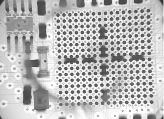
X-Ray Inspection
Meaning: Primarily used to inspect the quality of solder joints hidden beneath the chip, such as those in BGA (Ball Grid Array) and CSP packages, which are invisible to the naked eye.
Purpose: To detect defects such as short circuits, open circuits, cold solder joints, and excessive voids in the solder.
Depaneling
Meaning: PCB boards are usually designed as panels to improve production efficiency. After soldering, a depaneling machine (milling or cutting type) is used to separate the connected panels into individual PCBAs.
Purpose: To obtain individual products and avoid stress damage caused by manual depaneling.
AOI Inspection (Automated Optical Inspection)
Meaning: A high-resolution camera automatically scans the PCBA, comparing the captured components and solder joints with standard images in a database.
Purpose: To quickly detect visual defects such as missing components, incorrect components, reversed polarity, misalignment, solder bridging, and insufficient solder.
Third Stage: Board-Level Test & Post-Processing
Software Download / DL
Meaning: Firmware, operating system, and applications are programmed into the single board's memory using fixtures and interfaces (such as USB, JTAG).
Purpose: To give the single board its "soul," allowing it to run programs.
CT+SN (Cycle Test + Serial Number)
CT (Cycle Test): After software programming, the single board is repeatedly powered on and off for simple startup tests to screen out unstable products that fail early.
SN (Serial Number Writing): A unique serial number is written to a specific area of the software, binding the software to the hardware identity.
Meaning:
FT (Functional Test)
Meaning: This is the most comprehensive test. The single board is connected to a functional test fixture, simulating real-world usage scenarios, to test whether all interfaces (USB, audio, network, etc.), functions, and performance indicators meet design specifications.
Purpose: To ensure that every single board is a fully functional and qualified product. MMI (Man-Machine Interaction Test) | (First Article Inspection of Single Board)
Human-Machine Interaction Test: Tests interactive functions such as screen, buttons, touchscreen, and indicator lights.
First Article Inspection: At the beginning of mass production, a very detailed full-function inspection and verification is performed on the first or first few boards coming off the production line to ensure that the production line settings are correct before mass production can begin.
Meaning: Usually has two interpretations, but in this context, the latter is more likely:
Phase 4: Final Assembly & Quality Check
Thermal Pad Attachment / Shield Cover Installation
Thermal Pad: A thermal pad is attached to high-heat generating chips (such as CPU, power chips) to ensure good contact with the heat sink or casing, assisting in heat dissipation.
Shield Cover: A metal shield cover is attached to form a Faraday cage, shielding against electromagnetic interference (EMI) and ensuring the stable operation of sensitive circuits (such as RF units) on the board.
Meaning:
Visual Inspection
Meaning: Final manual visual inspection by a quality inspector.
Purpose: To check for defects that machines might miss, such as scratches, stains, lifted components, or dents in the shield cover, ensuring a perfect product appearance.
Board Storage
Meaning: After all processes are completed, qualified PCBA boards are labeled with a qualified tag, processed, and sent to the warehouse for storage, awaiting subsequent assembly into complete machines or shipment.
Purpose: The end of the process, completing production.
Summary Flowchart
This process reflects the high degree of automation, precision, and traceability in modern electronics manufacturing. Each step is an important link in ensuring the high quality and reliability of the final product.


