Development Prospects of HDI Printed Circuit Boards
AbstractHigh-density interconnect (HDI) printed circuit boards (PCBs) are a key carrier for the upgrading of the electronic information industry, and are core components supporting the miniaturization of consumer electronics, the high-speed development of communication systems, and the high-density computing infrastructure. This paper takes the global and Chinese HDI PCB industry from 2020 to 2026 as the research object, systematically reviewing its technological evolution path, market size changes, competitive landscape restructuring, and profound adjustments in downstream application structures. Research shows that the global HDI PCB market size has grown from US$9.4 billion in 2020 to US$12.8 billion in 2024, and is expected to reach US$16.9 billion by 2029. Among them, high-end HDI products have a significantly higher growth rate than low-end products, with a compound annual growth rate of 9.3% from 2020 to 2024, and is expected to further increase to 9.9% from 2025 to 2029. The artificial intelligence computing revolution, automotive electronics and intelligence, and the increasing penetration rate of foldable screens are the core driving forces for the continued expansion of HDI PCB demand. China has become the world's most important HDI board production base, accounting for 63% of global output in 2024. Meanwhile, domestic manufacturers are accelerating their efforts to move from low-to-mid-range to high-end and Any-Layer HDI (ALHDI), with leading companies such as Shenghong Technology, Pengding Holdings, and Shanghai Electric Group, Key Technology emerging as internationally competitive players in AI high-performance computing PCBs and high-end HDI. In the future, the HDI board industry will evolve towards higher frequencies, higher speeds, and higher densities, driven by material system innovation, the widespread adoption of mSAP semi-additive processes, and continuous increases in the number of layers and layers. This will lead to a simultaneous increase in industry value and technological barriers.
I. Introduction
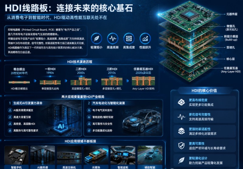
1.1 Research BackgroundPrinted Circuit Boards (PCBs) are hailed as the "mother of electronic products," serving as the physical carrier for electrical interconnection in almost all electronic devices. As the global electronics and information industry continues to evolve towards "lighter, thinner, smaller, faster, higher frequency, and higher integration," traditional PCBs have gradually reached their limits in terms of wiring density, signal integrity, and packaging compatibility. HDI (High-Intensity Distributed) circuit boards, as a core solution to meet the needs of next-generation terminal forms and high-performance computing, are increasingly demonstrating their strategic importance.
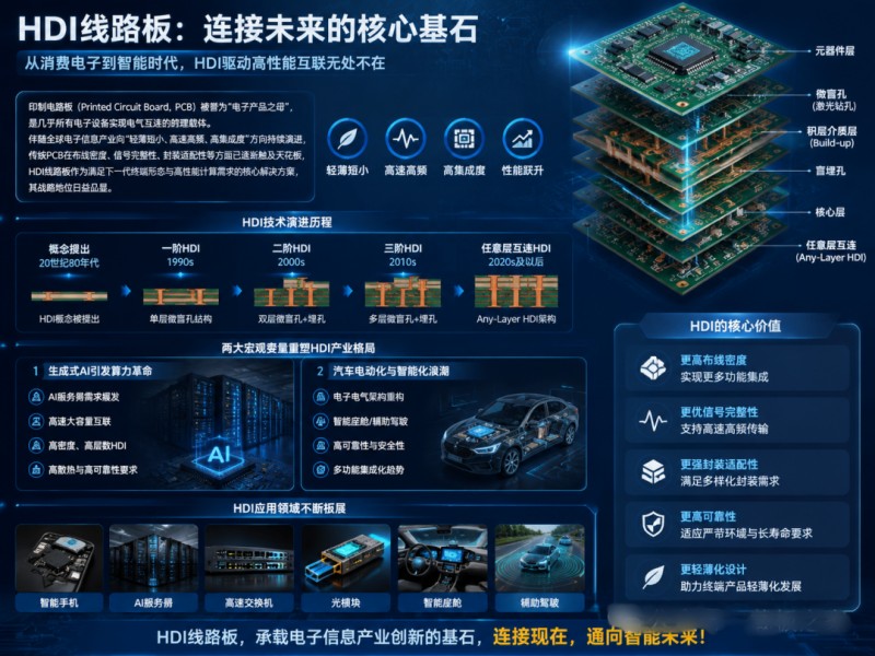
Since the concept of HDI was proposed in the 1980s, the technology has undergone continuous iterations through laser microvia, blind via, and build-up processes, gradually transitioning from early first-order products to second-order, third-order, and even Any-Layer HDI. Entering the 2020s, two major macroeconomic variables have profoundly reshaped the HDI industry landscape: the computing power revolution triggered by generative artificial intelligence, and the restructuring of automotive electronic architecture brought about by the electrification and intelligentization of vehicles. Against this backdrop, HDI boards have expanded from the single stage of traditional smartphone motherboards to a wide range of application scenarios, including AI servers, high-speed switches, optical modules, smart cockpits, and advanced driver-assistance systems.
1.2 Research Significance Given that mainland China has become the world's largest PCB manufacturing base, in-depth research on the current development status and future prospects of the HDI (High-Intensity Distributed) circuit board industry is of great significance in the following aspects: First, it provides a reference for understanding the technological competition path of the global electronics and information industry; second, it provides decision-making basis for domestic PCB companies to achieve breakthroughs in high-value-added fields such as high-end HDI and arbitrary-layer HDI; third, it provides an analytical framework for investors to identify structural opportunities in the process of industrial upgrading; and fourth, it provides a reference for policymakers to promote domestic substitution in areas such as electronic basic materials and precision manufacturing equipment.
1.3 Research Methodology This paper adopts a combination of literature review, industry data analysis, and industry case study methods. Data sources include publicly available data from third-party research institutions such as Prismark, Guanyan Report Network, Taoyue Consulting, QYResearch, and Frost & Sullivan, as well as publicly disclosed operating information and technological progress of major domestic HDI/PCB listed companies, striving to present an objective and quantitative industry picture.
II. Technical Connotation and Classification System of HDI Circuit Boards
2.1 Technical Definition of HDI Circuit Boards
HDI circuit boards, short for High-Density Interconnect Boards, are a type of high-end printed circuit board manufactured using a multilayer method. They utilize laser-drilled microvias, blind vias, and buried vias as core interconnection methods, achieving a wiring density far exceeding that of traditional PCBs. Their core characteristics include: miniaturized apertures (laser-drilled hole diameters are typically between 0.07 and 0.13 mm), refined line width/spacing (compressible to 0.0762 mm or even 20 μm/20 μm levels), and three-dimensional interlayer interconnections. Through processes such as the modified Semi-Additive Process (mSAP), the signal transmission capacity per unit area of HDI boards can be increased by more than 300% compared to traditional PCBs. They are mainly used in smartphone motherboards, 5G base station RF modules, AI server accelerator cards, and automotive electronic controllers. From a manufacturing process perspective, traditional PCBs use a subtractive process, while HDI introduces laser drilling for microvias and stacked vias on top of the subtractive process, reducing the minimum line width/spacing to 40μm. Due to yield bottlenecks in processes below 30μm, the process has further shifted to semi-additive (mSAP) and additive (SAP) processes, involving more copper plating steps, which places significantly higher demands on copper plating capacity, exposure equipment (more complex processes), and bonding equipment (more layers).
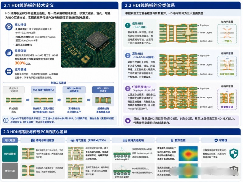
2.2 Classification System of HDI Circuit Boards Based on the complexity and order of the multilayer stacking process, HDI boards can be divided into three main types: (1) Low-order HDI: Primarily uses single-layer stacking (1-N-1 structure), with interlayer interconnection involving only single blind vias. Manufacturing difficulty is relatively controllable, and it is mainly used in low-to-mid-range consumer electronics products. (2) High-order HDI: Uses double or higher stacking (2-N-2, 3-N-3, etc. structures), involving multiple blind via stacking, misalignment, and cross-layer conduction. Process complexity is significantly increased, and it is widely used in high-end smartphones, tablets, and wearable devices. (3) Any-Layer HDI (ALHDI): Has the highest process complexity and best performance. Any layers can be directly interconnected via laser microvias, possessing the highest degree of wiring freedom and density, representing the current pinnacle of HDI technology. Currently, Any-Layer HDI has extended to 6-layer (24 layers), 10-layer (30 layers), and even 16-layer Any-Layer HDI technology capabilities, representing the industry's most advanced manufacturing capabilities. 2.3 Core Differences Between HDI Circuit Boards and Traditional PCBs Compared to traditional multilayer PCBs, HDI boards have significant advantages in electrical performance, structural density, and reliability: First, by replacing mechanical through-holes with laser-drilled micro-vias, they save PCB wiring area and significantly increase component density; second, they shorten interlayer interconnect lengths, reduce parasitic inductance and capacitance, and improve radio frequency interference, electromagnetic interference, and electrostatic discharge (RFI/EMI/ESD); third, they support finer BGA package pitch (≤0.4mm pitch), adapting to advanced packaging requirements; fourth, the dense micro-via structure is more conducive to vertical heat conduction in high-power scenarios such as AI servers, optimizing the heat dissipation capacity of local hot spots.
III. Current Status of the Global HDI Circuit Board Industry
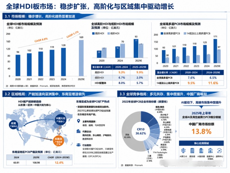
3.1 Steady Market Expansion, High-End Products Leading Growth The global HDI board market showed a steady expansion trend between 2020 and 2024. According to data compiled by Prismark and Guanyan Report, the global HDI board market size was approximately US$9.4 billion in 2020, growing to US$12.8 billion in 2024, with a CAGR of approximately 8.0%. Looking ahead, the global HDI board market size is projected to reach US$16.9 billion by 2029, with a CAGR of approximately 5.7% from 2024 to 2029. Notably, behind the overall moderate growth of the HDI board market, product structure upgrades are accelerating. Driven by the development of the AI industry, the global trend towards high-end HDI boards is significant: the CAGR of high-end HDI boards globally from 2020 to 2024 has surpassed that of low-end HDI boards, reaching 9.3%; it is projected that the CAGR of the global high-end HDI market size will further increase to 9.9% from 2025 to 2029, significantly outpacing the overall growth rate of the HDI board market. This structural change indicates that the value increment in the HDI industry is concentrating on high-end products with high technological barriers and high added value. In the high-multilayer PCB sub-market related to HDI boards, the AI-driven high-end trend is also evident. The global high-multilayer PCB market grew from US$9.3 billion in 2020 to US$12.5 billion in 2024, and is projected to reach US$17.1 billion in 2029, representing a CAGR of 6.5% from 2024 to 2029. The market size of 14-layer and above high-multilayer PCBs reached US$5.6 billion in 2024, with a CAGR of 9.5% from 2020 to 2024. This CAGR is expected to further accelerate to 11.6% from 2024 to 2029, demonstrating a multiplier effect of both increased volume and price in demand for high-end PCBs and HDI boards from high-performance computing equipment.
3.2 Regional Landscape: Accelerated Concentration of Production Capacity in Asia
From a global perspective, the HDI board production landscape has undergone a structural shift over the past two decades, moving from Europe and the US to Asia, and then to mainland China. Among major PCB manufacturers in Europe and the US, most HDI production capacity has shifted to Asia, except for a few companies like ASPOCOM and AT&S that still produce some second-order HDI mobile phone boards. Currently, mainland China, Taiwan, South Korea, and Japan constitute the core forces of global HDI board supply, with mainland China having the highest proportion.
Regarding specific regional investment trends, influenced by international trade frictions and geopolitical risks, since 2023, leading global PCB companies have tended to expand their production capacity in Southeast Asia. Countries like Thailand, Vietnam, and Malaysia, with their well-developed infrastructure, preferential policies, and controllable costs, have attracted leading domestic manufacturers, including PENGDING HOLDING, DONGSHAN MIUI, HUANGYUAN TECHNOLOGY, and SENGHONG TECHNOLOGY, to establish factories there. According to GPCA/SPCA statistics, 33 of the world's top 40 PCB companies have announced plans to establish production bases in Southeast Asia by 2026. According to Prismark's forecast, the PCB output value in Southeast Asia will reach approximately US$6.081 billion in 2024, a year-on-year increase of 8.4%; it is projected to reach US$10.898 billion by 2029, with a compound annual growth rate of 12.4% from 2024 to 2029, higher than other regions globally.
3.3 Global Competitive Landscape: Diversified Coexistence, Increasing Concentration
Similar to the overall PCB industry, the global HDI board market is relatively fragmented. In 2022, the CR10 of global PCB companies was approximately 36.62%, with leading manufacturers mainly from Taiwan (Zhen Ding/Peng Ding, Unimicron, etc.), mainland China (Dongshan Precision, Shennan Circuits, Hudian Technology, Shenghong Technology, etc.), Japan (Qisheng, Ibiden, etc.), the United States (TTM Technologies), and South Korea (Samsung Electro-Mechanics, Daedeok Electronics, etc.). In recent years, with the rise of high-end applications such as AI servers, industry concentration has been slowly increasing, with leading companies possessing high-end HDI mass production capabilities rapidly expanding their market share.
According to Frost & Sullivan data, in the first half of 2025, Chinese manufacturers, ranking first globally in the AI and high-performance computing PCB segment, achieved a market share of 13.8%, with core applications covering key equipment such as AI computing cards, servers, AI servers, data center switches, and general-purpose substrates. This data indicates that Chinese manufacturers have taken a leading position in high-end HDI application scenarios.
IV. Current Status of China's HDI Circuit Board Industry
4.1 Market Size: Consecutive Double-Digit Growth
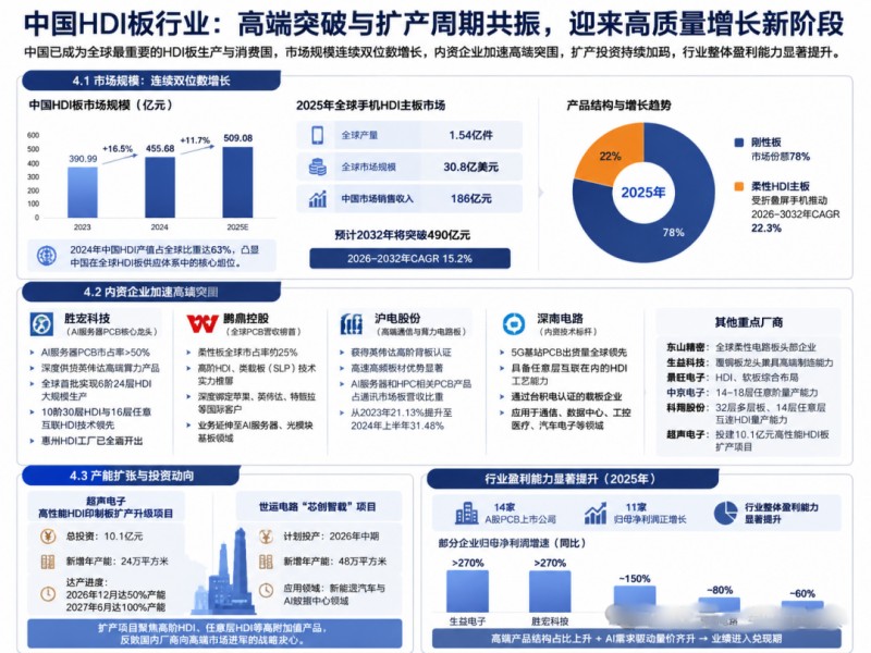
China has become the world's most important producer and consumer of HDI boards. Data shows that in 2024, the Chinese HDI board market size reached 45.568 billion yuan, a year-on-year increase of 16.5%; in 2025, the market size further climbed to 50.908 billion yuan, a year-on-year increase of 11.7%, maintaining double-digit growth for two consecutive years. It is worth noting that in 2024, China's HDI output accounted for 63% of the global total, highlighting China's core position in the global HDI board supply system.
From a segmented market perspective, mobile phone HDI motherboards are the largest application segment. According to data from Taoyue Consulting, the global output of HDI motherboards for mobile phones reached 154 million units in 2025, with a global market size of approximately US$3.08 billion. As the global manufacturing center for smartphones, China's HDI motherboard market revenue reached RMB 18.6 billion in 2025 and is projected to exceed RMB 49 billion by 2032, with a CAGR of 15.2% from 2026 to 2032, far exceeding the global average. In terms of product structure, rigid boards accounted for 78% of the market share in 2025, while flexible HDI motherboards, driven by foldable screen phones, are expected to achieve a CAGR of 22.3% from 2026 to 2032, becoming a new growth engine for the industry.
4.2 Domestic Enterprises Accelerate High-End Breakthrough
China's HDI board industry is showing a clear transformation from "scale growth" to "quality improvement." Leading domestic enterprises are breaking the long-standing technological monopoly of manufacturers from Taiwan, Japan, and South Korea in the high-end HDI field by continuously increasing R&D investment and technological breakthroughs.
(1) Shenghong Technology: As a core leader in AI server PCB, its market share of AI server PCB-related products exceeds 50%. It deeply supplies NVIDIA with high-end computing power products, and its 800G and 1.6T optical module substrate technology is leading. It continues to expand its production overseas to undertake computing power orders. The company focuses on high-end HDI and high-multilayer PCB fields, and has taken the lead in breaking through the core technology barrier of combining high-multilayer and high-end HDI. It has the manufacturing capability of high-multilayer boards with more than 100 layers and is one of the first companies in the world to achieve large-scale production of 6-level 24-layer HDI products, as well as 10-level 30-layer HDI and 16-layer arbitrary interconnection HDI technology capabilities. The Huizhou HDI factory will be fully operational by 2025, and it has a high degree of synergy with major overseas customers in HDI products. (2) PENGDING HOLDING: The world's leading PCB manufacturer and consumer electronics flexible circuit board company, with a global market share of approximately 25% for flexible boards. It possesses strong technical capabilities in high-end HDI and Substrate-Like PCB (SLP). Its product range covers multiple categories including FPC, SMA, SLP, HDI, Mini LED, RPCB, and Rigid Flex. It has deep partnerships with international clients such as Apple, NVIDIA, and Tesla, and its business extends to AI servers and optical module substrates.
(3) HUYUAN TECHNOLOGY: Deeply involved in high-end communication and computing circuit boards, it has obtained NVIDIA's high-end backplane certification and holds a prominent market share in the North American AI server market. Its high-speed, high-frequency board materials have significant advantages. Since launching the HDI project with an estimated output value of RMB 1.98 billion in 2021, the company has accelerated the HDI technology upgrade project with an estimated output value of RMB 550 million in January 2024. As a major supplier of AI products for long-term cooperation with major overseas customers, the proportion of its AI server and HPC-related PCB products in the company's enterprise communication market board revenue increased from 21.13% in 2023 to 31.48% in the first half of 2024.
(4) Key Technology: A domestic technology benchmark, leading the world in 5G base station PCB shipments, capable of mass-producing ultra-high layer number circuit boards; its PCB business has HDI process capabilities including arbitrary layer interconnection, mainly used in communications, data centers, industrial control, medical, automotive electronics and other fields; at the same time, it is one of the few domestic carrier board companies certified by TSMC.
4.3 Capacity Expansion and Investment Trends
From the perspective of recent industrial investment, China's HDI board industry is in a new round of capacity expansion cycle. In December 2025, Ultrasonic Electronics announced a planned investment of 1.01 billion yuan in a high-performance HDI printed circuit board capacity expansion and upgrade project. Upon completion, it will add 240,000 square meters of annual production capacity, with 50% capacity expected to be reached by December 2026 and 100% by June 2027. World Circuit's "Core Innovation and Intelligent Carrier" project is planned to commence production in mid-2026, adding 480,000 square meters of annual capacity, primarily targeting the new energy vehicle and AI data center sectors. These expansion projects generally focus on high-value-added products such as high-end HDI and arbitrary-layer HDI, reflecting the strategic determination of domestic manufacturers to enter the high-end market. In terms of profitability, among the 14 A-share listed PCB companies that have released their performance reports in 2025, 11 saw positive growth in net profit attributable to the parent company, with Shengyi Electronics and Shenghong Technology both exceeding 270% growth, indicating a significant improvement in the overall profitability of the industry. This trend suggests that Chinese HDI companies are entering a period of performance realization, benefiting from both the increasing proportion of high-end products and the simultaneous increase in both volume and price driven by AI demand.
V. Downstream Application Landscape and Demand-Driven Analysis
5.1 Application Structure: From Consumer Electronics Dominance to Diversified Expansion Around 2020, mobile terminals held an absolute dominant position in the downstream applications of HDI boards. According to Prismark statistics, in 2020, mobile terminals, PCs, other consumer electronics, and automobiles accounted for 58.1%, 14.5%, 11.7%, and 5.7% of the global HDI downstream applications, respectively. However, since 2023, with the rise of AI servers and high-performance computing, and the rapid penetration of automotive intelligence, the HDI application structure is undergoing profound changes, presenting a more diversified landscape. While mobile terminals still account for the largest share, the contributions of emerging scenarios such as AI servers, data centers, automotive electronics, and wearable devices have significantly increased.
5.2 Mobile Phone Motherboards: A Stable Foundation Although the overall global smartphone shipments have leveled off, the penetration rate of HDI boards in mobile phone motherboards continues to increase, and the value per unit continues to rise due to the trend towards higher-end products. Modern smartphones, with a body thickness of less than 8mm, simultaneously house multiple cameras, high-performance processors, and 5G RF modules, all relying on HDI motherboard technology. Compared to traditional PCBs, HDI motherboards offer higher wiring density, superior electrical performance, and stronger integration capabilities, perfectly matching the development trend of smartphones towards "thinness, high performance, and multi-functionality," making them a standard feature in high-end phones. The rise of foldable phones has opened up new growth opportunities for HDI boards. By 2025, Huawei's market share in the domestic foldable phone market reached 69%, and global foldable phone shipments increased by 80% year-on-year, with penetration expected to exceed 20% by 2030. As a core component of foldable phones, the demand for flexible HDI motherboards will continue to surge.
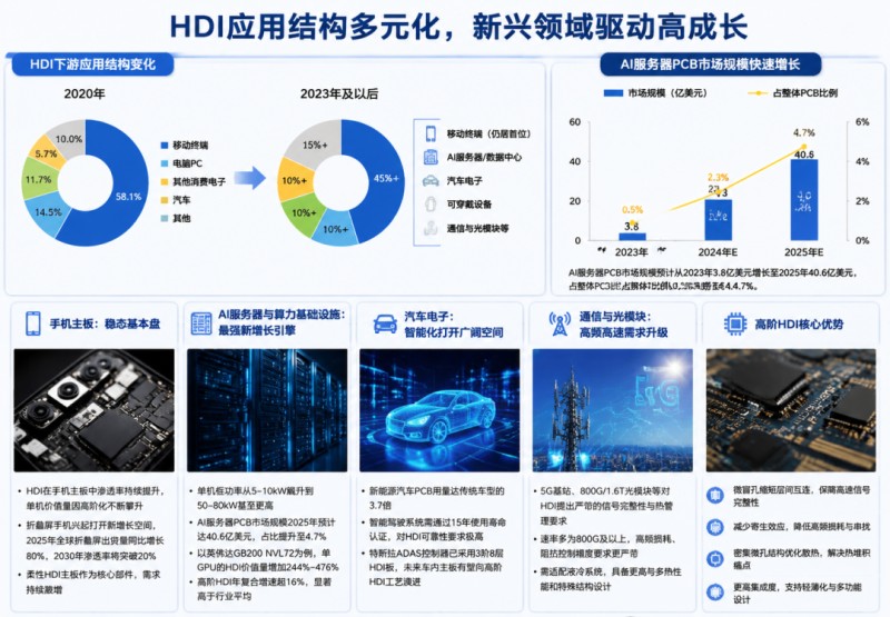
5.3 AI Servers and Computing Infrastructure: The Strongest New Growth Engine. The most direct impact of the AI megamodel is the surge in single-rack power from the traditional 5-10kW to 50-80kW or even higher, with GPU density doubling, bandwidth leaping, and signal rates reaching 112Gbps and 224Gbps. Traditional PCBs struggle to meet this challenge, making high-end HDI the core carrier for AI terminals and accelerator cards. In terms of volume, the market size of AI server PCBs is projected to grow from $380 million in 2023 to $4.06 billion in 2025, with its share of the overall PCB market rising from 0.5% in 2023 to 4.7% in 2025. From the perspective of unit value, taking the NVIDIA GB200 NVL72 as an example, it adopts the NVLink 5.0 protocol (with a bandwidth of 1800Gbps), which significantly increases the transmission rate requirements compared to NVLink 4.0, making it more suitable for HDI with higher signal transmission rates. Compared to the DGX series, the HDI value of a single GPU in the GB200 NVL72 increases by 244%–476%. According to data from 2023 to 2028, the compound annual growth rate of high-end HDI for AI servers exceeds 16%, significantly higher than the average growth rate of the PCB industry, placing it in a leading position among all PCB subcategories. High-speed signal integrity constraints are the fundamental reason why high-end HDI is indispensable in AI servers. With the popularization of high-speed interconnect protocols such as PCIe 5.0 and NVLink, signal transmission rates have exceeded 32GT/s, and excessively long signal paths are prone to attenuation, crosstalk, and impedance runaway problems. High-end HDI micro-vias significantly shorten inter-layer interconnect lengths, reduce parasitic inductance and capacitance, lower high-frequency losses, and ensure stable data interaction for multi-GPU interconnect clusters over extended periods. Simultaneously, the dense micro-via structure facilitates vertical heat conduction, optimizes local hotspot heat dissipation on the motherboard, and addresses the pain point of heat buildup in high-density layouts.
5.4 Automotive Electronics: Intelligentization Opens Up Vast Opportunities. New energy and intelligent connected vehicles are driving a structural expansion in demand for HDI boards. New energy vehicles use 3.7 times more PCBs than traditional vehicles, and intelligent driving systems require 15-year lifespan certification, placing extreme demands on the reliability of HDI boards. Tesla's ADAS controller already uses a 3rd-order, 8-layer HDI board, and future in-vehicle motherboards are expected to follow a similar evolution path to mobile phone motherboards, moving from low-end to high-end HDI processes. From vehicle domain controllers to driver assistance/autonomous driving systems, from smart cockpits to millimeter-wave radar, an increasing number of automotive electronic applications require high-speed computing chips within a limited volume, providing a continuously growing market for HDI boards. 5.5 Communication and Optical Modules: Continuously Upgrading High-Frequency and High-Speed Demands High-frequency and high-speed communication equipment such as 5G base stations and 800G/1.6T optical modules place stringent requirements on HDI boards for signal integrity and thermal management. Optical module PCBs for AI servers have even higher performance requirements, with speeds mostly at 800G and above, demanding stricter requirements for high-frequency loss and impedance control accuracy; stronger heat dissipation requirements necessitate adaptation to liquid cooling systems, requiring PCBs with higher thermal conductivity and special structural designs; and a high degree of customization, requiring adjustments to PCB layout based on different computing chip architectures, resulting in more complex interface designs. Furthermore, AI servers place higher reliability requirements on PCBs, requiring longer periods of testing in high and low temperature environments and vibration.
VI. Technological Evolution Trends and Process Changes
6.1 Continuously Increasing Order: From Low-Order HDI to Arbitrary Layer Interconnection The main thread of HDI technology evolution is the continuous increase in order and layer count. The industry development path is clearly presented as follows: ordinary PCB → first-order HDI → second-order HDI → third-order HDI → any-layer HDI → higher-order any-layer HDI. In high-end application scenarios, fourth-order and above any-layer HDI can complete high-density wiring in extremely small spaces, and has become a core solution for AI terminals and accelerator cards. Currently, leading companies have mass-produced sixth-order 24-layer HDI and have the technical capabilities for 10-order 30-layer HDI and 16-layer any-layer HDI.
6.2 Material System Upgrade: Low Dk/Df Becomes the Focus of Competition. The performance ceiling of a PCB is determined by the substrate material by approximately 90%. The PCB speed competition in the AI era is essentially a material speed competition. High-speed signals are most vulnerable to loss, and the industry generally uses dielectric constant (Dk) and dielectric loss factor (Df) as core indicators to measure material performance. Low Dk/Df materials can allow 224Gbps signals to run smoothly throughout the entire process, avoiding attenuation and distortion. This is also the core reason why leading domestic copper clad laminate manufacturers such as Nanya New Materials and Shengyi Technology are striving to reach the M9 and M10 high-end materials level – only by obtaining the ticket to high-end materials can they truly enter the AI supply chain. Specific material directions include: (1) Resin: from ordinary epoxy to high-speed and high-frequency systems, the penetration rate of PTFE substrate in 5G base stations has reached 40%, the dielectric constant has dropped to below 2.2, and the signal loss has been reduced by 25%; (2) Copper foil: HVLP (Hyper Very Low Profile) copper foil is accelerating its localization; (3) Glass cloth: low dielectric electronic cloth is constantly iterating and upgrading; (4) Filler material: low coefficient of thermal expansion (CTE) filler meets complex stress environment.
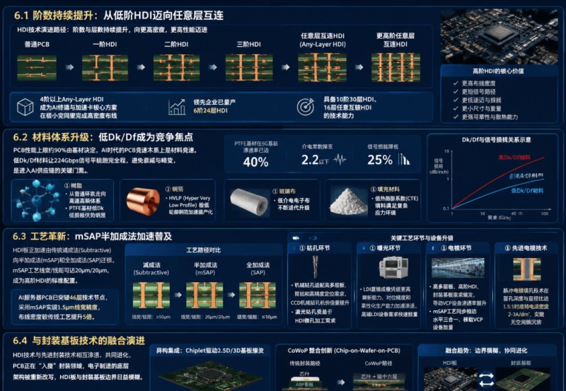
6.3 Process Innovation: mSAP Semi-Additive Method Accelerates Popularization At the process level, HDI boards are accelerating their migration from the traditional subtractive method to the semi-additive method (mSAP) and the super-additive method (SAP). With its more refined line width/spacing control capabilities (which can compress line width to 20μm/20μm level), mSAP has become the standard configuration for high-end HDI. AI server PCBs have broken through the 46-layer technology node and use the semi-additive method (mSAP) to achieve a line width accuracy of 1.5μm, with a wiring density 5 times higher than the traditional process. In specific stages: (1) Drilling stage: Mechanical drilling needs to adapt to the requirements of high multilayer boards, back drilling and high-precision positioning, and the value of CCD mechanical drilling machines has increased; laser drilling benefits from the demand for HDI micro-hole processing. (2) Exposure stage: LDI direct imaging is accelerating its penetration with higher resolution, alignment accuracy and flexible production capabilities, and the demand for high-end LDI equipment is rapidly increasing. (3) Electroplating process: The explosive growth in demand for high-multilayer boards, high-end HDI, and packaging substrates has driven the increased penetration rate of VCP equipment. Simultaneously, mSAP technology has promoted the mass production of horizontal three-in-one and transfer VCP equipment. Pulse electroplating filling technology maintains a current density of 2-3 A/dm² when the blind via depth-to-diameter ratio reaches 1.5:1, achieving void-free copper deposition.
6.4 Integration and Evolution with Packaging Substrate Technology: HDI technology is mutually penetrating and evolving with advanced packaging technologies. In terms of heterogeneous integration technology, Chiplet packaging has driven the explosive growth of 2.5D/3D substrates, and TSV (Through Silicon Via) technology has increased interconnect density by 100 times, integrating over 100,000 TSV vias on a single substrate. Even more disruptive is CoWoP (Chip-on-Wafer-on-PCB) technology—skipping the traditional ABF carrier board and directly placing the chip and silicon interposer on the PCB, shortening the signal path, reducing latency, and compressing costs. This signifies that PCBs are beginning to "invade" the packaging field, rewriting the underlying architecture of electronic manufacturing and blurring the lines between HDI boards and packaging substrates.
VII. Core Challenges Facing the Industry
7.1 High-End HDI Technology and Capacity Barriers High-end HDI production lines have extremely high investment barriers, with equipment investment exceeding one billion yuan per line. They require sophisticated processes such as picosecond laser drilling, in-hole plating, and semi-additive mSAP, making it difficult for small and medium-sized manufacturers to enter the market. This high capital and technology barrier has led to the global high-end HDI market being dominated by overseas and Taiwanese companies for a long time. Mainland Chinese manufacturers need a long investment cycle and customer certification process to increase their market share in the high-end market.
7.2 Yield Control Challenges The increase in the number of layers and order in HDI boards brings an exponential increase in process complexity. The more layers, the more difficult it is to achieve interlayer alignment, lamination accuracy, and impedance control. Every percentage point improvement in yield requires extensive optimization of process details. Fluctuations in process yield, high material costs, and the risk of thermal stress delamination remain the main bottlenecks for the mass production of high-end HDI.
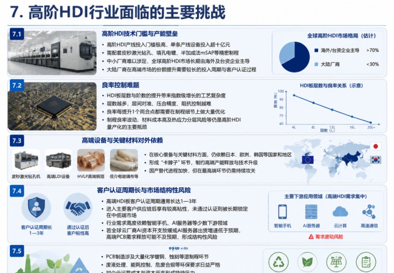
7.3 Dependence on Foreign Suppliers for High-End Equipment and Key Materials Although China leads the world in HDI/PCB manufacturing capacity, it still relies to some extent on suppliers from Japan, Europe, and South Korea for core equipment such as picosecond laser drilling machines, high-end LDI direct imaging equipment, and precision bonding equipment, as well as key materials such as HVLP high-end copper foil, low-dielectric glass cloth, and high-performance copper-clad laminates, creating bottlenecks. While the process of domestic substitution is accelerating, continuous efforts are still needed in the highest-end segments.
7.4 Long Customer Certification Cycles and Structural Market Risks The customer certification cycle for high-end HDI boards typically lasts 1-3 years. Once a product enters the supply chain of a major customer, it enjoys high customer loyalty. Conversely, manufacturers that fail to obtain certification are locked into the low-to-mid-end market for a long period. At the same time, industry demand is highly dependent on a few downstream sectors such as smartphones and AI servers. If global cloud vendors slow down their AI capital expenditures or AI server shipments grow slower than expected, the demand for high-multilayer PCBs, HDI, and high-speed, high-frequency boards may fall short of expectations, creating structural risks. 7.5 Environmental Protection and Sustainable Manufacturing Pressures PCB manufacturing involves numerous wet processes such as chemical copper plating and etching. Increasingly stringent environmental requirements regarding wastewater treatment, energy consumption control, and hazardous waste compliance place continuous pressure on companies' operating costs and capital expenditures. Leading manufacturers need to continuously increase investment in green manufacturing, wastewater reuse, and clean energy.
VIII. Future Development Prospects
8.1 Market Space: Strong Certainty of Structural Growth Overall, the global HDI board market will maintain steady expansion over the next five years, with high-end HDI boards showing significantly faster growth. The global HDI board market size is projected to reach US$16.9 billion by 2029. As the world's largest production base and consumer market, China's market size is expected to continue expanding at a double-digit rate, with the Chinese mobile phone HDI motherboard market size expected to exceed RMB 49 billion by 2032. The overall size of the domestic HDI board industry will also continue to climb, driven by multiple factors such as AI servers, automotive electronics, and the high-end development of consumer electronics. 8.2 Technological Upgrade: Arbitrary Layer Interconnection and Ultra-High Order Become the Mainstream Direction The future evolution of HDI technology will revolve around the following directions: (1) The order will be further improved, and HDI with arbitrary layer interconnection of 10th order or above will gradually achieve mass production; (2) The line width/line spacing will continue to be refined, and 20μm/20μm will become the standard configuration of high-end products, with some products challenging the 10μm level; (3) The material system will evolve towards low Dk/Df, high heat resistance, and high reliability; (4) The automation and intelligence of the process links will be improved, and AI-assisted process optimization and digital twin production lines will be accelerated; (5) HDI boards will be integrated with emerging technologies such as packaging substrates and glass substrates to form new composite forms.
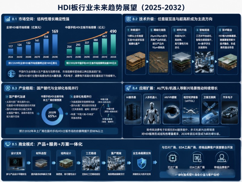
8.3 Industry Landscape: Domestic Substitution and Globalization in Parallel Over the next five years, China's HDI board industry will exhibit a two-way evolution characterized by "accelerated domestic substitution and parallel globalization." On the one hand, with leading domestic manufacturers achieving technological breakthroughs in high-end HDI and any-layer HDI, domestic mid-to-low-end HDI motherboards have achieved full domestic substitution, while the high-end market still has significant room for growth; it is projected that by 2032, domestic manufacturers will hold over 65% of the domestic mobile phone HDI motherboard market share. On the other hand, to mitigate the risks of international trade frictions, leading domestic manufacturers are accelerating their investment and factory establishment in Southeast Asia (especially Thailand and Vietnam), building a "mainland China + Southeast Asia" dual-base structure.
IX. Policy Recommendations and Investment Implications
9.1 Policy Level
Firstly, further increase support for the R&D and industrialization of high-end PCB specialized equipment (picosecond laser drilling machines, high-end LDI equipment, precision electroplating equipment, etc.) to address shortcomings in equipment supply.
Secondly, support technological breakthroughs in key basic materials such as high-end copper-clad laminates, HVLP copper foil, low-dielectric glass cloth, and special electronic resins through national major science and technology projects.
Thirdly, promote talent cultivation in interdisciplinary fields such as electronic circuits, materials, and precision machining through higher education and vocational education to alleviate the shortage of professional talent in the industry.
Fourthly, encourage leading enterprises to invest across borders and operate in compliance with regulations to help them mitigate trade friction risks and expand into international markets.
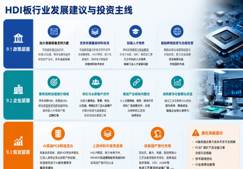
9.2 At the Enterprise Level: First, focus on high-value-added niche markets such as high-end HDI, any-layer HDI, and ultra-high-performance multilayer boards to avoid falling into the red ocean of overcapacity in the low-to-mid-end market. Second, strengthen joint R&D and deep partnerships with leading downstream customers (such as NVIDIA, Apple, Huawei, BYD, and Tesla) to secure orders in high-growth sectors like AI servers and smart cars in advance. Third, emphasize vertical integration of the industry chain, achieving synergistic optimization from materials to processes through strategic cooperation with upstream material manufacturers such as copper clad laminates, copper foil, and glass cloth. Fourth, accelerate digital and intelligent transformation, improving yield and reducing costs through the Industrial Internet and AI-powered quality inspection.
9.3 Investment Perspective For investors, the HDI board industry presents three main investment themes: First, leading AI high-end PCB manufacturers possessing technological barriers in high-multilayer boards and advanced HDI, having entered the supply chains of top clients like NVIDIA, and directly benefiting from the explosive growth in AI server demand; second, beneficiaries of upstream material upgrades, including companies achieving domestic substitution of high-end materials such as HVLP copper foil, low-dielectric electronic cloth, and M9/M10 high-speed copper-clad laminates; and third, pioneers in domestic equipment substitution, namely equipment manufacturers with leading technologies in core process equipment such as drilling, exposure, electroplating, and etching, capable of meeting the requirements of advanced processes such as high-multilayer boards, HDI, and mSAP. At the same time, investors should also pay attention to potential risks such as lower-than-expected capital expenditures on AI servers and computing power, lower-than-expected expansion of PCB manufacturers and fulfillment of equipment orders, changes in technology routes, and intensified industry competition.
X. Conclusion
As a key carrier for the upgrading of the electronic information industry, the development of HDI circuit boards reflects the profound transformation of the global electronics manufacturing industry from "standardized production" to "high-precision manufacturing." Currently, the HDI industry has shifted from a single-driven model of traditional consumer electronics to a multi-engine driven pattern of "stable consumer electronics foundation + explosive growth in AI computing power + structural expansion in automotive electronics," with industry growth momentum shifting from quantitative expansion to value enhancement. From a technological perspective, HDI boards are continuously evolving towards "higher order, finer linewidth, lower loss, and stronger heat dissipation." Any-layer interconnect HDI, low Dk/Df material systems, and mSAP semi-additive processes constitute the three major technological pillars of the next generation of products. From an industry perspective, mainland China has become the most important manufacturing base for the global HDI board industry. Leading domestic companies are rapidly narrowing the gap with international advanced levels in cutting-edge fields such as high-end HDI, any-layer HDI, and ultra-high multilayer boards, and have already achieved a global leading position in the AI high-performance computing PCB segment. Looking ahead, with the continued penetration of emerging applications such as artificial intelligence, intelligent vehicles, foldable screens, robotics, and satellite internet, the HDI board industry will usher in structural growth opportunities in the next 5-10 years. Whether China's HDI industry can seize this window of opportunity to achieve a historic leap from "scale leadership" to "technology leadership" depends on the continuous efforts of leading companies in core technologies, key equipment, and basic materials, as well as on collaborative innovation across the industrial chain and strong policy support. It is foreseeable that, as the "invisible heart" of the AI computing era and the "neural network" of the Internet of Things era, HDI circuit boards will play an even more crucial role in the restructuring of the electronics and information industry landscape in the next decade.