Why Do Chips Get Damaged by "Static Electricity"? A Guide to Understanding ESD, HBM, MM, and CDM Models
If you have worked on IC projects, testing, packaging, or failure analysis (FA), or have handled customer-reported field failures, you have likely heard this statement:
"This device might have been damaged by ESD."
But what exactly is ESD?
Why can a touch from a person, contact with equipment, or even a small residual charge on the chip itself cause internal circuitry to fail? What scenarios do the three industry-standard models—HBM, MM, and CDM—actually simulate?
In this article, rather than diving straight into complex ESD protection circuits, we will start with the fundamentals:
What is ESD? Why are chips vulnerable to it?
What are the differences between the HBM, MM, and CDM models? How is ESD robustness tested in an engineering context?
1. ESD is more than just "getting a shock"
ESD stands for Electrostatic Discharge.Static electricity is ever-present in daily life. Walking on the ground, friction between clothes, or the contact and separation of plastic materials can all lead to the accumulation of static electricity. Often, the accumulated voltage is high enough to threaten integrated circuits long before a person feels any sensation.
For instance, walking on plastic flooring in an environment with about 40% humidity can generate static voltages of several kilovolts (kV) or even over ten kV; yet, a person typically only clearly perceives a "shock" when the voltage exceeds a few kV.
In other words, many ESD events occur without the person even noticing.
For a chip, the danger stems not only from "high voltage" but also from several critical characteristics:
Extremely short duration,
Very high current,
Highly concentrated energy release, and
Vulnerability of localized structures.
When static charge—accumulated either from the external environment or within the chip itself—flows into or out of the chip through a pin, the resulting instantaneous current and voltage can cause two typical types of damage.
The first type is electrical breakdown.
Examples include gate oxide breakdown caused by high electric fields, PN junction breakdown due to abnormal reverse bias, and sudden increases in device leakage current; in severe cases, this leads to direct short circuits or open circuits.
The second type is thermal damage.
When a massive instantaneous current flows through localized metal traces, contact vias, diffusion regions, or parasitic devices, intense localized heating occurs. This can cause metal traces to melt, silicon to burn, and junction regions to sustain damage, potentially resulting in permanent failure. This is precisely why ESD poses such a challenge for ICs:
It can occur at any stage—manufacturing, packaging, shipping, assembly, testing, or end-user operation. The event is extremely brief and does not necessarily result in immediate, total failure; often, the root cause can only be determined through failure analysis by correlating the location of the damage with electrical performance characteristics.
Therefore, ESD is not merely a matter of a simple "zap"; it is a systemic issue involving charge accumulation, transient discharge, localized current paths, and device reliability.
2. Why establish ESD models?
Electrostatic discharge (ESD) occurs in many forms in nature and in manufacturing environments; it is impossible to replicate every real-world scenario exactly within a laboratory setting.From an engineering perspective, what is truly needed includes:
Repeatable test conditions; comparable test results; definable pass/fail criteria; and classification levels suitable for product quality control.
Consequently, the industry abstracts common ESD scenarios into distinct models, then uses test equipment to generate corresponding pulses and apply them to the device under test.
Here is a common acronym: DUT.
DUT stands for "Device Under Test."
Regarding ESD in integrated circuits (ICs), the three most common models are:
HBM: Human Body Model;
MM: Machine Model;
CDM: Charged Device Model.
These three acronyms essentially address three different questions:
What happens when a person carrying a static charge touches a chip? What happens when a machine or metal conductor carrying a static charge touches a chip? What happens when a chip itself is charged and then comes into contact with a ground?
Once these three concepts are understood, it becomes much easier to grasp ESD standards, testing methods, failure analysis, and protection circuits.
3. HBM: A charged person touching a chip
HBM stands for Human Body Model.It simulates a scenario that is very easy to visualize:
A human body accumulates static electricity through activities such as walking or friction. When a person handles, operates, or touches a semiconductor device, the charge on the body enters the device through a specific pin and subsequently flows out via a grounding path.
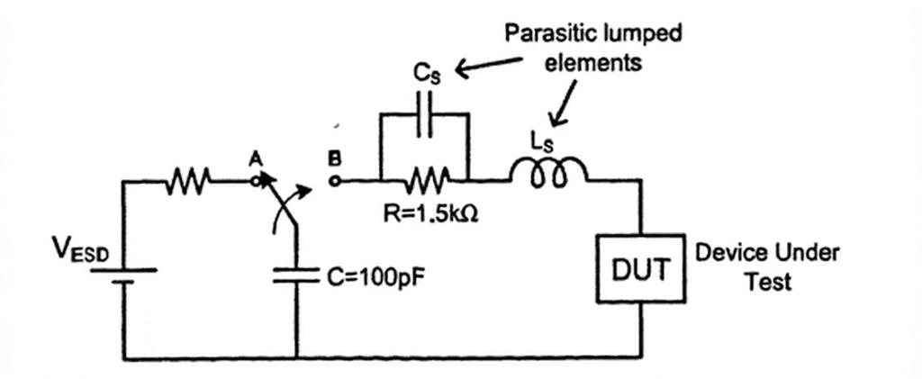
Figure 1.1 can be drawn as the equivalent circuit of the HBM.
In the HBM equivalent circuit, the human body is typically modeled as a capacitor and a discharge resistor. Typical parameters include:
Human body equivalent capacitance: 100 pF; human body equivalent discharge resistance: 1500 Ω; factors such as parasitic inductance and capacitance within the test system are also taken into account.
Due to the relatively high series resistance, the HBM discharge waveform is not as extremely narrow or sharp as that of the CDM; however, it can still generate a significant transient current.
Taking a typical HBM waveform as an example, a 2 kV HBM ESD pulse has a peak current in the order of 1 A, a rise time typically in the nanosecond range, and a pulse duration that can reach the order of hundreds of nanoseconds.
From an engineering management perspective, HBM corresponds to risks associated with "people."
For example:
Are personnel correctly wearing anti-static wrist straps? Are anti-static shoes, bench mats, and grounding connections effective? Are tasks such as handling samples, inserting/removing boards, or operating sockets performed within an EPA (Electrostatic Protected Area)? Are bare ICs, boards, or samples being casually placed on ordinary plastic bags, foam, or paper?
A simple way to remember HBM:
A charged person touches the chip.
For layout engineers, the key takeaway regarding HBM is that the ESD current path must be continuous, low-impedance, and sufficiently wide. Protection devices near the pad, power-to-ground clamps, metal trace widths, the number of vias, guard rings, and substrate pickups are not merely optional details.
Many ESD failures occur not because protection devices are missing from the schematic, but because the current path is too long, too narrow, or too convoluted, leading to localized burnout.
4. MM: A machine or metal object becomes charged and contacts the chip
MM stands for Machine Model.It simulates scenarios where conductive elements—such as machines, robotic arms, metal fixtures, or tools—accumulate static charge and subsequently discharge upon contacting IC pins.
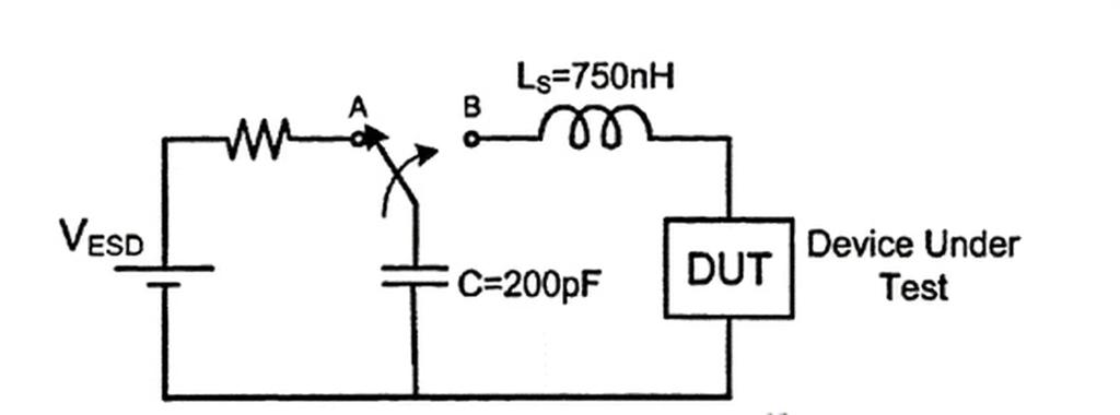
Figure 1.2 Equivalent circuit of the MM
In a typical MM model, the capacitance is set at 200 pF, and the series inductance in the discharge path is approximately 750 nH. Unlike HBM, MM lacks a large series discharge resistor (such as the 1500 Ω one found in HBM); consequently, it more closely resembles a low-impedance discharge process occurring when a metal conductor makes direct contact with a device.
This implies that the MM discharge can be more "severe," with peak currents more prone to concentration, thereby placing higher demands on local current paths and the uniformity of device triggering.
However, a point worth adding here is:
While MM was historically a very common ESD model, its importance in many current device-level ESD qualification standards has diminished relative to HBM and CDM. We discuss MM today primarily to help illustrate a specific type of risk: a charged, low-impedance metal conductor coming into contact with a chip.
In terms of on-site management, issues associated with MM typically include:
Whether metal fixtures are reliably grounded; whether there are floating metal parts on robotic arms, probes, or clamps in automated equipment; whether there are points of abnormal discharge in test sockets, load boards, handlers, or tray transport paths; and whether makeshift tools or structural modifications have compromised the original grounding design.
A simple way to remember MM:
A machine or metal conductor becomes charged and touches the chip.
From an engineering operations perspective, the key takeaway from MM is not that "every product must achieve a high MM rating," but rather:
Do not focus solely on personnel. Equipment, fixtures, metal tools, and automated mechanisms can equally serve as sources of ESD risk.
5. CDM: The chip itself becomes charged and discharges outward
CDM stands for Charged Device Model.Its directionality is the exact opposite of HBM and MM.
In HBM and MM, an external object becomes charged and then contacts the chip.
In CDM, the chip itself becomes charged first and then discharges to an external conductor through one of its pins.
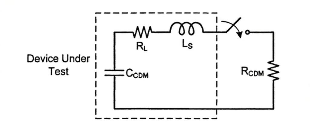
Figure 1.3 Equivalent circuit of CDM
This scenario is critical in automated production, packaging, material handling, and testing.
For instance, as an IC moves through tubes, trays, pick-and-place nozzles, handlers, and test equipment, it can accumulate an electric charge due to friction, induction, or environmental factors. At this stage, the chip is charged but has not yet discharged.
Once a pin makes contact with a grounded metal surface, the accumulated internal charge may rapidly discharge through that pin.
The danger of CDM can be summarized in two words:
Fast and sharp.
CDM pulses feature extremely short rise times and potentially high peak currents, with discharge occurring along a highly localized path. CDM poses a particular threat to advanced process technologies, small-geometry devices, thin gate-oxide structures, and pads lacking adequate local discharge paths.
Taking a typical 500 V CDM waveform as an example, the discharge current rise time can be in the sub-nanosecond range, and the peak current can reach several amperes or higher. Specific values depend on factors such as package size, the device's equivalent capacitance, the test environment, and the discharge path.
In other words, while the CDM test voltage may appear lower than that of HBM, the current rise rate is extremely rapid, resulting in a violent localized surge.
A simple way to remember CDM:
The chip itself holds a charge and discharges instantly upon touching a ground.
For layout engineers, the implications of CDM are crucial:
One cannot rely solely on a distant, global power clamp.
There must be a local discharge path near the pad that is sufficiently fast, short, and characterized by low resistance and low inductance. Otherwise, the CDM current might damage small local components before the remote clamp can even react.
6. Waveform differences among the three models
HBM, MM, and CDM differ not only in name but also significantly in their waveforms.
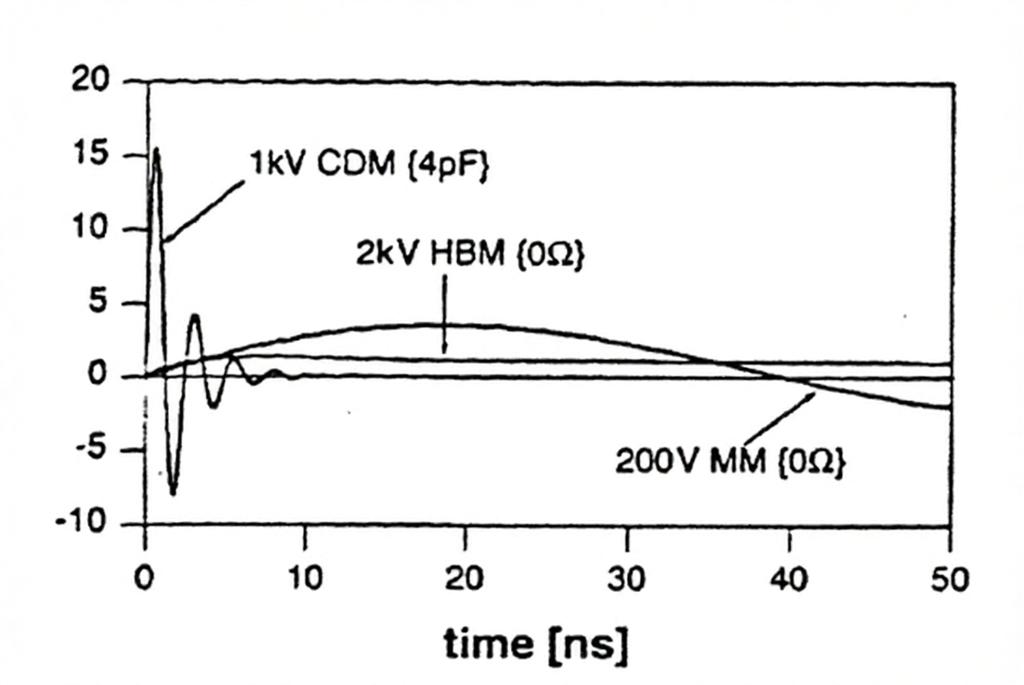
Figure 1.4 Discharge current waveforms for HBM, MM, and CDM.
The HBM waveform is relatively broad with a longer duration; the energy release process closely mimics the discharge from a charged human body.
The MM model features lower source impedance, resembling a discharge from a metal conductor, resulting in a more direct current surge.
The CDM pulse is the narrowest with the fastest rise time and potentially very high peak current, making it particularly prone to causing localized damage.
To understand this through engineering intuition:
HBM is akin to "a person touching the chip."
MM is akin to "a metal tool or piece of equipment touching the chip."
CDM is akin to "the chip itself becoming charged and suddenly finding a discharge path."
7. ESD testing is not limited to just "a single pin."
ESD testing is based on pin combinations.Because ESD current does not necessarily follow the path we intend, it seeks out the discharge path with the lowest actual impedance and easiest trigger conditions among various pins, power rails, ground lines, I/O ports, and internal structures.
Therefore, ESD testing cannot simply assess the robustness of an individual pin; instead, tests must be conducted using various combinations.
Common test combinations fall into three categories.
Category 1: Testing each I/O pin against VSS or VDD.
This involves using the ground line (VSS) or power line (VDD) as a reference point and applying a positive or negative stimulus to the I/O pin under test. This typically encompasses four modes:
PS: Positive to VSS;
NS: Negative to VSS;
PD: Positive to VDD;
ND: Negative to VDD.
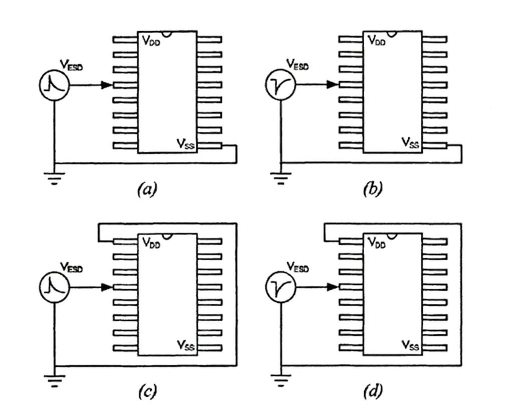
Figure 1.5 illustrates several test modes for I/O-to-power line testing.
Type 2: I/O-to-I/O testing.
The I/O pin under test is connected to the stimulus, while the remaining I/O pins are grounded and VSS/VDD are left floating; this is done to observe whether the discharge path between I/O pins is safe.
Type 3: Power rail testing.
This refers to testing between VDD and VSS. It corresponds to a critical structure in chip-level ESD protection: the power clamp.
This illustrates why chip ESD protection involves more than simply placing a diode next to a specific pin.
Actual ESD current can enter through any pin and exit via another power rail, ground line, I/O pin, or substrate path. The essence of ESD design lies in proactively establishing a safe, low-impedance, and robust pathway for these currents.
8. HBM/MM/CDM tests look at ratings; TLP looks at curves.
HBM, MM, and CDM tests generally answer a pass/fail question:Does the device continue to function correctly at a specific test voltage?
For instance, HBM testing determines whether a product meets 2 kV or 4 kV ratings, while CDM testing uses specific voltages to evaluate a device's CDM protection capability.
However, for ESD design engineers, knowing merely whether a device "passed" or "failed" is insufficient.
We also want to know:
When does the protection device trigger? Can the voltage be clamped to a low level after triggering? What is the on-resistance under high current? At what current level does failure occur? How does the leakage current change before and after failure?
This is where TLP comes in.
TLP stands for Transmission Line Pulsing.
Unlike HBM, MM, and CDM tests—which directly simulate specific natural discharge scenarios—TLP uses repeatable, controllable pulses to observe the I-V characteristics of ESD devices under high-current conditions.
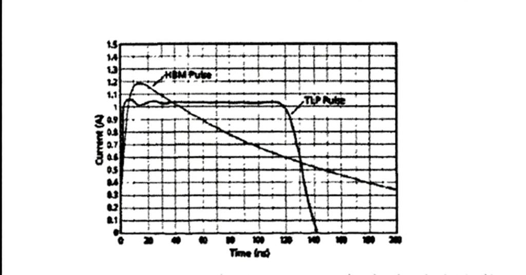
Figure 1.6 Comparison of TLP and HBM current waveforms.
TLP testing typically involves incrementally increasing the pulse amplitude while monitoring the device's leakage current before and after each pulse application. The device is considered to have failed when the leakage current significantly degrades and exceeds a preset threshold.
The value of TLP lies in its ability to reveal the key parameters of ESD devices to engineers.
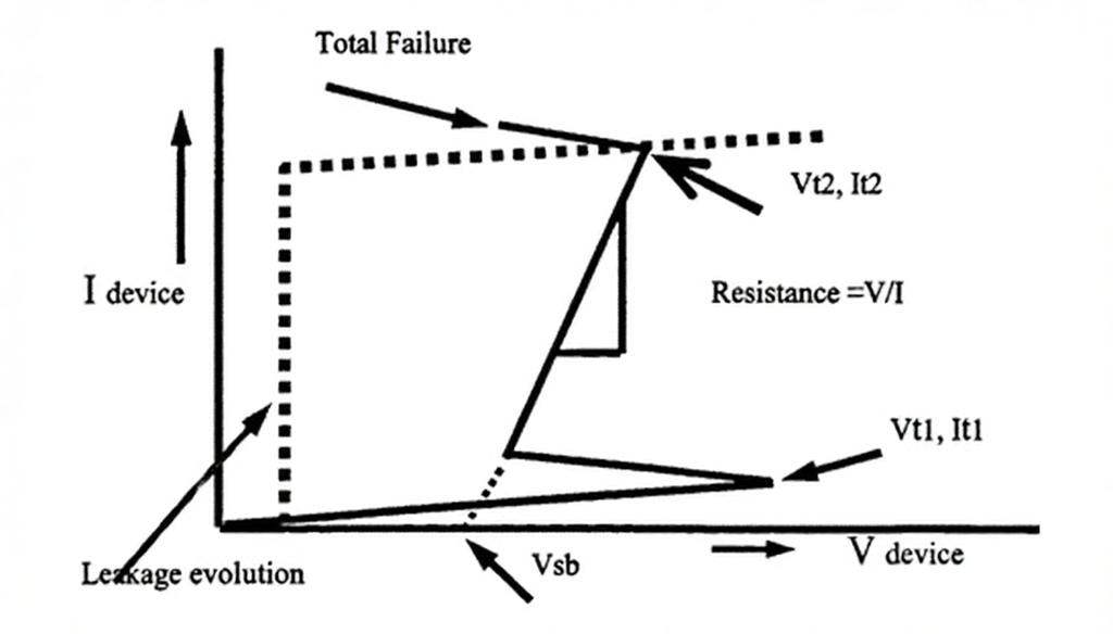
Figure 1.7 shows a typical TLP I-V curve.
Several parameters are particularly important:
Vt1: Trigger voltage;
It1: Trigger current;
Vh or Vsp: Holding voltage;
Ron: On-resistance;
Vt2: Failure voltage;
It2: Failure current.
Simply put:
An ESD protection device must remain off during normal operation so as not to interfere with the chip's function; when an ESD event occurs, it must activate rapidly to shunt the high current away; once activated, it must clamp the voltage seen by the internal circuitry to a low level; and it must withstand as much current as possible before failing itself.
Therefore, HBM, MM, and CDM are more akin to product-level qualification tests, whereas TLP serves more as a design analysis tool.
One answers the question "Can it pass the rating?", while the other helps us understand "Why did it pass or fail?" and "Where is the point of greatest vulnerability?"
9. Summary: How do we distinguish between the three models?
In this article, we first clarify the fundamental concepts of ESD.ESD is not merely a question of whether a person gets a shock; rather, it concerns the instantaneous flow of electrostatic charge into or out of chip pins, which can cause issues such as gate oxide breakdown, junction damage, and localized metal overheating.
The differences between HBM, MM, and CDM can be summarized in three sentences:
HBM: A charged person touches the chip.
MM: A charged machine or metal conductor touches the chip.
CDM: The chip itself is charged and discharges upon touching an external conductor.
Regarding testing methods, two sentences suffice:
HBM/MM/CDM testing is primarily used to evaluate whether a device can meet a specific rating under standard models.
TLP testing is primarily used to analyze the complete I-V characteristics of ESD devices, helping engineers understand the processes of triggering, discharging, holding, and failure.
For IC projects, the real value lies not in memorizing three acronyms, but in being able to reverse-engineer the source of risk when encountering real-world issues.
Is the risk associated with human contact? That points to HBM. Is it contact with equipment, fixtures, or tools? That points to MM. Is it charge accumulation on the device itself during handling or automated processes? That points to CDM.
Once this is understood, looking at ESD protection circuits—such as power clamps, I/O protection, and the trade-offs involving parasitic capacitance in RF circuits—goes far beyond the simplistic notion of merely "adding a protection device." ESD is not merely a matter concerning a single component; rather, it is the result of the combined influence of pads, protection circuits, power networks, ground return paths, substrate connections, metal trace widths, via counts, and system usage scenarios.