
The copper on the chip pins is exposed after soldering. What could be the reason?
The copper on the chip pins is exposed after soldering. What could be the reason?
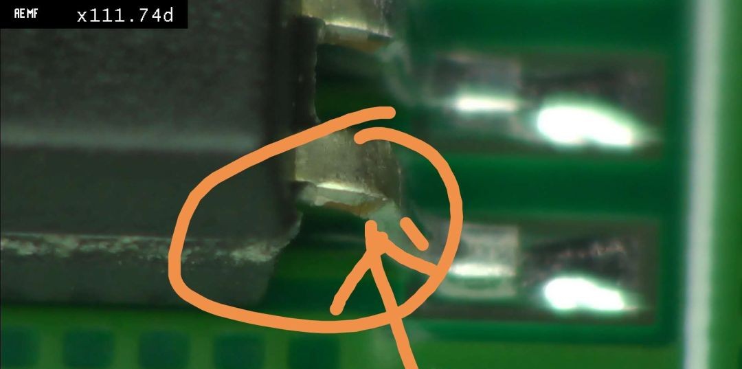
Question: I want to ask an expert. The pins of the chip are suspected to be exposed after welding? What could be the reason?
george tsao: The pins in the photo are normal. They are like this after packaging.
Lin Gong: The roots of the tube pins are all bare copper, right? @george tsao
george tsao: The material of Lrad Frame for IC packaging is copper surface with plating. It is etched before packaging or punched after packaging to cut out the component legs, causing the copper base material on the side of the component legs to be exposed @林工
Lin Gong: Is this normal?
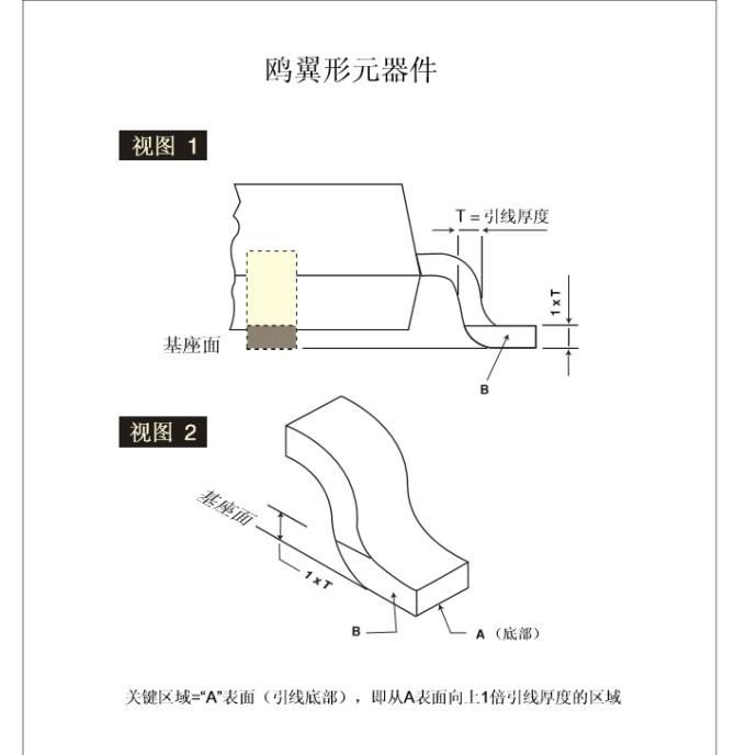
Liu Haiguang: There is no impact on the solderability. Generally, superficial defects in the coating of the IC bracket can be tolerated... The exceptions are whether there are cracks in the base material of the inner and outer curved surfaces and where the solder climbs and where the solder dissolution will cause cracks. The expansion needs to be separately evaluated@林工
Liu Haiguang: An additional question is whether there is a transition layer between the surface coating and the pin base material. This determines the reliability of the welding. Additional evaluation can also be done on the peeled off coating@lin gong
george tsao: The side is acceptable, just like the front of the toes, but if it is the sole of the foot, it is not acceptable @lingong
Lin Gong: It’s close to the side, and it’s the upper part of the pin. There should be no solder climbing here, and no cracks have been found @ Liu Haiguang, as shown below:
Liu Haiguang: Is it because the plating of the pins at the base of the body fell off and desoldered? Then it also depends on the quality of the solder joints in the AB welding area. Are there any pictures of the appearance of the solder joints in the original AB area? @lin gong
george tsao: Make sure there is no exposed copper on the top and bottom of the pin. Make sure it is only the side that is exposed due to cutting. But if it is also on the top and bottom of the pin, it may be that the plating is not done properly and may even deteriorate @lin gong
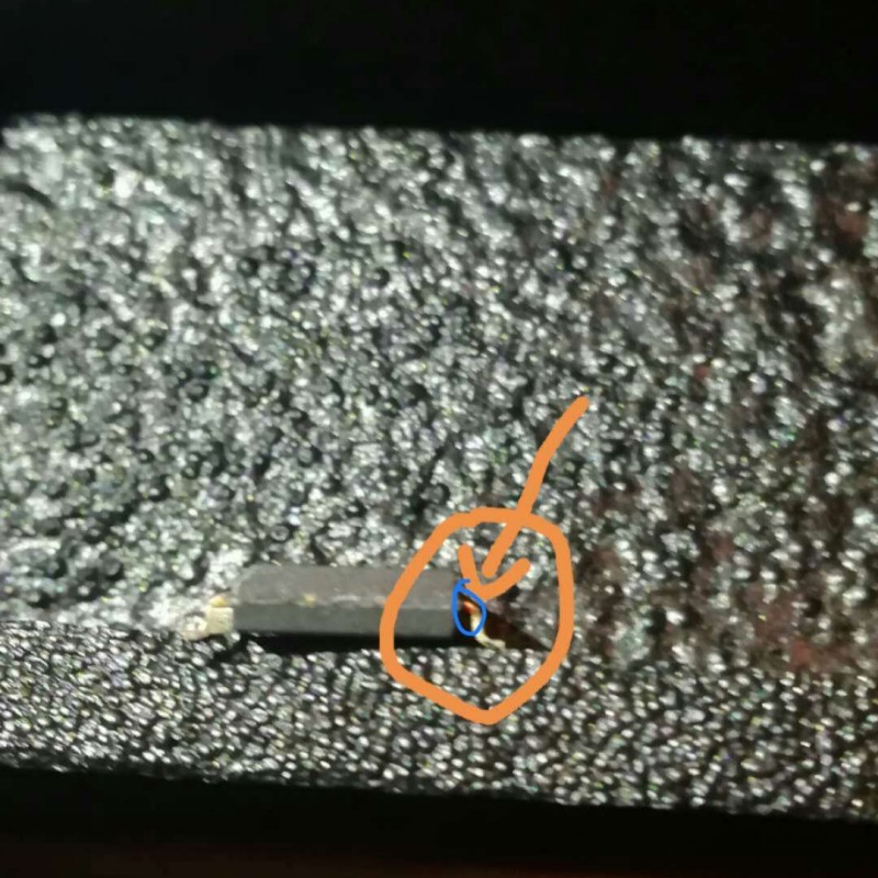

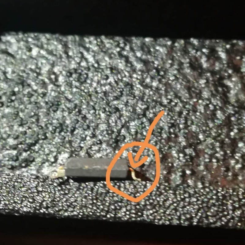
george tsao: The front side cannot be seen in the photo. However, the problems in these two photos should be different. The latter photo shows normal exposed copper, but the former one may have damaged the plating during the packaging molding process. It may also have damaged the upper and lower surfaces of the pins.
Lin Gong: These two photos have different camera equipment and angles. They are all related to one device and one problem. Thank you, I think the coating is not plated @george tsao
george tsao: The photo that looks more reddish copper is not clear. Should the two photos be in the same position or the same sentence? If it is the upper and lower surfaces of the parts, the plating is not done well. If it is the side, it is acceptable to have different positions. s reason


