
Popularization: one second to read the electronic components packaging
Packaging means that the circuit pins on the silicon wafer are connected to the external connector with wires in order to connect with other devices; the package form refers to the housing used to install the semiconductor integrated circuit chip.It not only plays a role in the installation, fixation, sealing, protection of the chip and enhance the electrical and thermal properties, but also through the contacts on the chip with wires connected to the pins of the package shell, these pins are connected to other devices through the wires on the printed circuit board, so as to achieve the connection between the internal chip and the external circuit.
Because the chip must be isolated from the outside world to prevent air impurities on the chip circuit corrosion and cause degradation of electrical performance. On the other hand, the encapsulated chip is also easier to install and transport.
I have organized a few types of electronic components common package, remember to collect the horse!
I, chip resistors / chip capacitors.
Industry buy and sell components often say 0805, 0201 package, for those who have just entered the industry and astronomical figures.In fact, the resistor-capacitor package is simply their size. To 0805 for example, SMD SMD components package size for the imperial 0805 surface mount devices, that is, the metric system 2012, said the component length = 2 mm width = 1.2 mm.
SMD SMD SMD components package size types.
Metric system: 3216 --- 2012 --- 1608 --- 1005 --- 0603 --0402.
Imperial: 1206 --- 0805 --- 0603 --- 0402 --- 0201 ---01005.
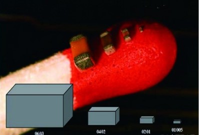
Since the early stages of surface assembly technology, the trend has been towards smaller and smaller passive and active components. The main driver for smaller components is portable products (cellular phones, laptops, PDAs, etc.). We now have the smallest passive component package, 01005 package.
II, SMD diodes.
Name, size and pad pitch, other package names of similar sizeSMC, 6.8X6-8.0
SMB, 4.5X3.5-5.3
SMA, 4.5X2.5-5.0, SOD-106
SOD-123, 2.7X1.6-3.5, SC-77A
SOD-323, 1.7X1.2-2.5, SC-76/SC-90A
SOD-523, 1.2X0.8-1.6, SC-79
SOD-723, 1.0X0.6-1.4
SOD-923, 0.8X0.6-1.0
III, the chip transistor:
the Name, size and pad pitch, other package names of similar size
D2PAK, 10X8.8-2.54, LDPAK
DPAK, 6.5X5.5-2.3, SC-63
SOT-223, 6.5X3.5-2.3, SC-73
SOT-89, 4.5X2.5-1.5, TO-243/SC-62/UPAK/MPT3
SOT-23, 2.9X1.5-2.0, SC-59A/SOT-346/MPAK/SMT3
SOT-323, 2.0X1.2-1.3, SC-70/CMPAK/UMT3
sot-523, 1.6x0.8-1.0, sc-75a/emt3
SOT-623, 1.4X0.8-0.9, SC-89/MFPAK
sot-723, 1.2x0.8-0.8
SOT-923, 1.2X0.8-0.8, VMT3
IV. IC chips/ICs.
1、SOP/SOIC package
SOP is the abbreviation of English Small Outline Package, that is, small outline package. SOP package technology was developed successfully by Philips in 1968-1969, and then gradually derived SOJ (J-type pin small outline package), TSOP (thin small outline package), VSOP (very small outline package), SSOP (reduced SOP), TSSOP (thin reduced SOP) (thin reduced SOP) and SOT (small form factor transistor), SOIC (small form factor integrated circuit), etc.2、DIP package
DIP is the abbreviation of English Double In-line Package, that is, double in-line package. DIP is one of the most popular cartridge package, the application range includes standard logic IC, memory LSI, microcomputer circuits, etc.3、PLCC package
PLCC is the abbreviation of Plastic Leaded Chip Carrier, that is, plastic J-lead chip package. PLCC package, square shape, 32-pin package, surrounded by pins, the form factor is much smaller than the DIP package. The advantages.4、TQFP package
TQFP is the abbreviation of Thin Quad Flat Package, which is a thin plastic sealed quad flat package. The Thin Quad Flat Package (TQFP) process makes effective use of space, thereby reducing the requirement for printed circuit board space size. Due to the reduced height and size, this package process is ideal for space-critical applications, such as PCMCIA cards and networking devices. Almost all of ALTERA's CPLD/FPGAs are available in TQFP packages.5、PQFP package
PQFP is the abbreviation of Plastic Quad Flat Package, the distance between the pins of the chip in PQFP package is very small and the pins are very thin, generally large-scale or super large-scale integrated circuits use this package form, the number of pins is generally above 100.6、TSOP package
TSOP is the abbreviation of the English Thin Small Outline Package, that is, the thin small size package. a typical feature of TSOP memory packaging technology is to make pins around the package chip, TSOP is suitable for SMT technology (surface mount technology) in the PCB (printed circuit board) to install wiring. TSOP package form factor, parasitic parameters ( When the current changes substantially, causing output voltage disturbance) is reduced, suitable for high-frequency applications, easier to operate, and more reliable.7、BGA package
BGA is the abbreviation of Ball Grid Array Package, that is, the ball grid array package. 1990s with the progress of technology, chip integration continues to improve, the number of I/O pins increased sharply, power consumption also increased, the requirements of integrated circuit packaging is also more stringent. In order to meet the needs of development, BGA packages began to be used in production.
The author of this article, focus on providing PCBA circuit board substitute material processing, SMT SMD, DIP plug-in processing, LED lighting production and electronic products assembly test inspection and the whole process services.
Adhering to the "excellence, quality wins" concept, the main customers belong to the electronic industrial control enterprises, the main management personnel are engaged in PCBA industry for more than 10 years. In the future, we will also take technological innovation as the main line, and constantly update the advanced production equipment to provide high quality and efficient professional services for our customers.


