
Why might a BGA pad fall off?
Why might a BGA pad fall off?
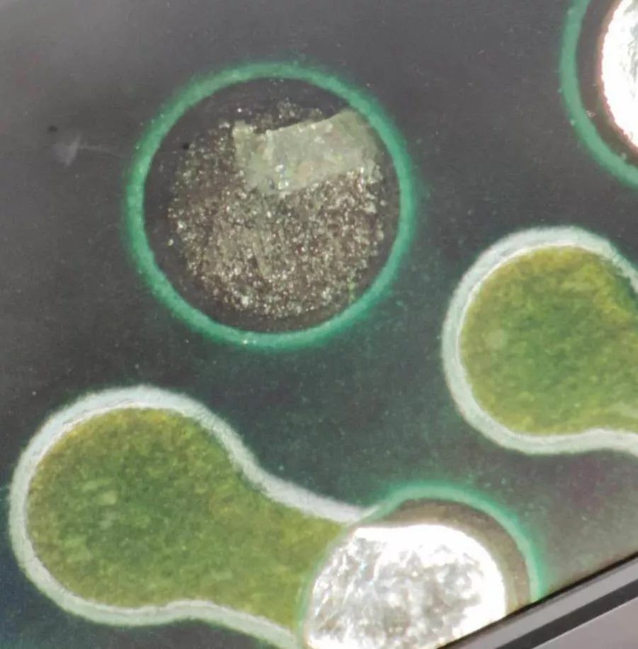
Wang Gong: Could you please help me analyze why the BGA pad may fall off? After one side of the board has been reflowed, but before the other side has been reflowed, it is found that there is an orphan pad without a solder pad. I don’t know which link it happened. As shown below:
Liu Haiguang: The desoldering temperature control was incorrect.
Engineer Wang: I haven’t soldered the components yet, so I discovered it. No desoldering
george tsao: This is a blank board. You can see it after reflowing one side first? The spray tin plate should have fallen off during the spray tin process. You didn't check it before you went online.
l Liu Haiguang: We should dehumidify it first. The copper foil area of the reactive pad is too small. Is there something wrong with this design? @wang gong
Liu Haiguang: Because you said it is an isolated pad, which is generally understood as an independent pad without electrical connection. I wonder if this is the case? @wang gong
Wang Gong: Yes, Teacher Liu
george tsao: Find a scrapped board, heat the pad like this, pull it out hard, and compare the surface, as shown below:
Wang Gong: What is the purpose @george tsao
Liu Haiguang: It doesn’t matter if it doesn’t fall off. I can’t think of increasing the copper foil area in addition to the solder mask opening. The purpose is to increase the adhesion strength of the copper foil.
george tsao: The connection between the base material and the copper foil may have changed before tin spraying@wang gong
Wang Gong: Will other pads also have this phenomenon? @george tsao
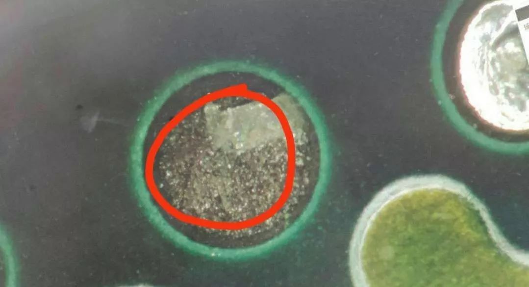
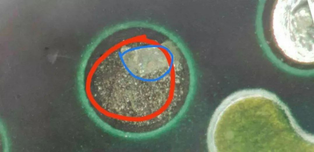
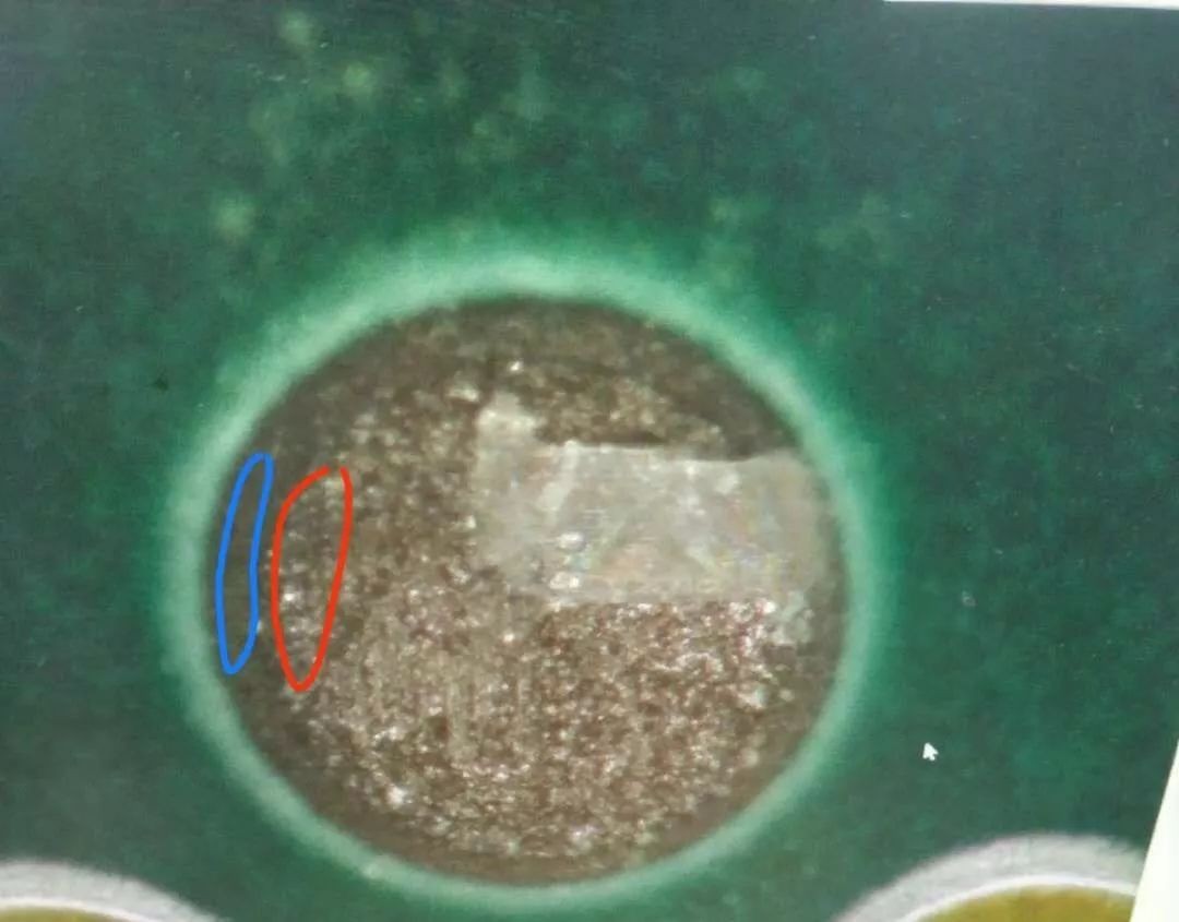
george tsao: Find the same board with the same non-functional independent pad, heat it with a soldering iron and push it gently to see if it will also fall off, and the three-dimensional condition cannot be seen. Is the position of the blue circle other impurities or a sunken base material? As shown below:
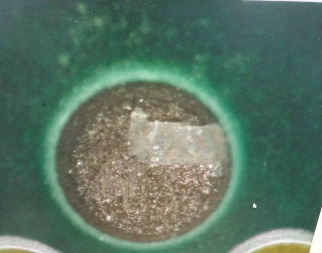
Wang Gong: As shown below:
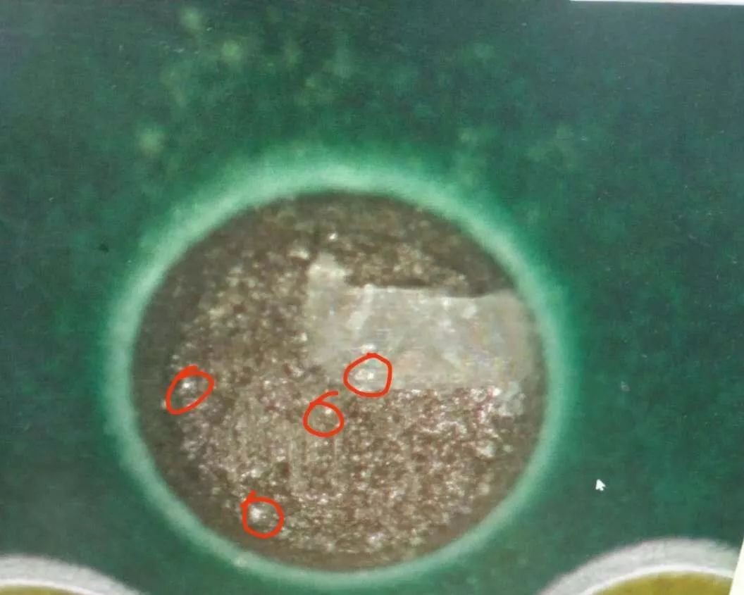
george tsao: Scratch the surface of the entire solder pad slightly and see. There seems to be a height difference between the two areas. I wonder if it is an illusion of the plane of the photo? As shown in the picture:
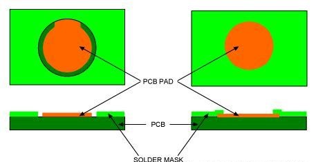
Liu Haiguang: Reactive pads are mostly used for welding reinforcement, but NSMD cannot be used for solder resist. SMD is fine, so it is a design error, as shown in the picture:
george tsao: Scratch the surface of the solder pad to see if it is confirmed that there is no copper pad residue at all. The red circle is after the pad falls off, the base material is stained with solder, and the solder is not sprayed off after spraying. There is a little tin on the entire surface of the solder pad.
george tsao: Another very likely situation is that the copper material in the joint area between the bottom of the pad and the base material has been severely oxidized before tin spraying. The flux attached before tin spraying even penetrates into the oxidized area to partially remove the oxide. Soldering pad spray tin Sometimes, the upper layer of the pad is eroded or peeled off, leaving the oxide layer below because it is partially cleaned by flux, so it barely gets some solder, so the pad area looks a bit different from the real base material area next to it.


