PCB Stack-up Design Related
Key Points of PCB Stack-up Design
I. Basic Concepts
1. What is a stack-up?
A PCB consists of multiple layers of copper foil and insulating dielectric material (FR-4 resin/glass fiber) laminated together.- Copper foil: Used for routing, ground planes, and power planes; provides electrical conductivity.
- Dielectric: FR-4 (insulating material); the dielectric surrounding the signal traces determines impedance, crosstalk, and heat dissipation.
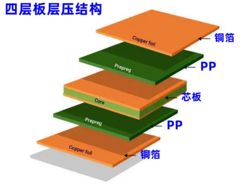
Stack-up = copper layer sequence + copper thickness of each layer + dielectric thickness + dielectric constant.
2. Key Parameters
1. Dielectric Constant Er (Dk)- Typical FR-4 value: 4.0–4.5.
2. Dissipation Factor Df (tan δ)
- Affects signal quality.
3. Copper Thickness (Oz)
- 1 oz ≈ 35 μm copper foil; 0.5 oz ≈ 17.5 μm; 2 oz ≈ 70 μm.
Copper thickness determines: current-carrying capacity, impedance calculations, and via current-carrying capacity.
4. Dielectric Thickness (h)
- The thickness of the insulating material between two copper layers (e.g., the dielectric thickness between a signal layer and a reference ground plane).
5. Characteristic Impedance (Z0)
- Single-ended 50Ω and differential 100Ω are the most common industry standards.
6. Differential Impedance (Zdiff)
- The combined impedance of a pair of tightly coupled differential traces. Differential 100Ω ≈ tightly coupled single-ended 50Ω traces.
7. Reference Plane (Reference Layer)
- The ground or power copper plane adjacent to the signal trace. Signals travel along surface or inner layers; while signal current flows along the copper trace, the return current must flow back via the nearest reference plane. Without a continuous reference plane, the return path is broken, EMC performance collapses, and impedance control is lost. This is the golden rule of stack-up design.
8. Return Path (Return Current)
- High-speed signal design involves more than just the trace itself; the return current is the key factor for EMC and signal integrity.
High frequency: Return current flows along the reference plane directly beneath the signal trace, following the path of least inductance.
If the reference plane is split or slotted, the return current is forced to take a longer detour, increasing the loop area and causing radiated interference to spike.
9. Prepreg (PP) vs. Core
- Core: A cured substrate with copper on both sides and a cured dielectric in the middle.
- PP (Prepreg): A semi-cured resin sheet that melts during lamination, bonding cores together and forming the interlayer dielectric.
II. Core Principles of Stack-up Design
Principle 1: Signal layers must be adjacent to a continuous reference plane (Ground is preferred; avoid using Power planes as references).
- Signal layer ↔ GND plane: Ideal configuration.
- Signal layer ↔ Power plane: Acceptable, but power planes often carry significant noise, so avoid using them as signal references whenever possible.
Principle 2: GND planes should be paired and close together; Power planes should closely follow GND planes.
- Tight coupling between Power and GND: Minimize the dielectric thickness between the Power and GND planes.
Principle 3: Symmetrical stack-up (Crucial).
- The stack-up structure must be symmetrical from top to bottom.

Symmetry: Copper thicknesses and dielectric thicknesses should be mirrored across the vertical axis. Asymmetric PCBs are prone to warping after lamination, deformation during SMT assembly, and soldering defects. The higher the layer count, the more critical symmetry becomes.
Principle 4: Outer Layers vs. Inner Layers
- Outer layers: Adjacent to air (Er ≈ 1); for a given trace width, impedance is higher than on inner layers;
- EMI from outer layers radiates more easily;
- Inner layers: Surrounded by dielectric material on both sides with uniform Er; better impedance control; lower radiation; but involves more vias.
Principle 5: Control interlayer thickness to suppress crosstalk
- For two signal layers sharing the same pair of reference planes, the dielectric thickness should be minimized;
- Avoid placing two signal layers directly facing each other; a ground plane must be inserted between them.
Principle 6: Prioritize cost; do not add layers unnecessarily
- Higher layer counts increase costs. Evaluate signal count, impedance requirements, power rail count, and EMC risks before determining the layer count.
III. Classic Stack-up Schemes for Common Layer Counts
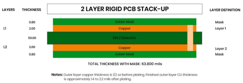
2-Layer Board (Low-cost, low-speed)Top (Signal) / Bottom (Signal)
- Disadvantages: Lacks a continuous reference plane; poor performance for high-speed signals; poor EMC. Suitable only for low-speed applications. Grounding relies on copper pours rather than a continuous plane.
4-layer board (most common)
Recommended: Top – GND – PWR – Bottom
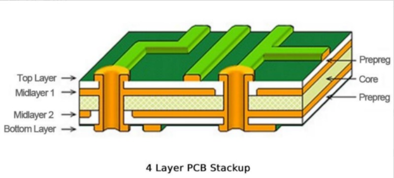
- Top: Signal; adjacent to GND reference;
- GND: Continuous ground plane;
- PWR: Power plane; positioned close to GND for good power coupling;
- Bottom: Signal;
- Advantages: Moderate cost; signals on both top and bottom layers have ground references; tight coupling between power and ground.
- Drawback: No internal signal layers; high-speed signal lines must be routed on the outer layers.
- Not recommended (4-layer): Top-Sig-Sig-Bottom. Two signal layers face each other without ground isolation, leading to crosstalk.
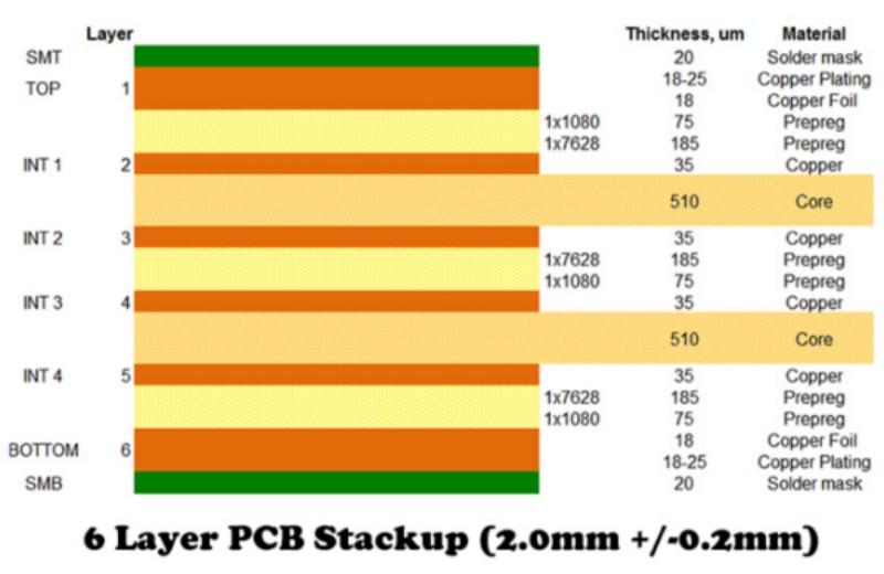
Preferred standard symmetrical 6-layer stackup:
Top(Sig) | GND | Sig1 | Sig2 | PWR | Bottom(Sig)
- Drawback: Signal layers Sig1 and Sig2 are directly adjacent without an intervening ground plane, creating a risk of crosstalk between them; routing on these two layers must be orthogonal (perpendicular).
Top(Sig) | GND | Sig | GND | PWR | Bottom(Sig)
- Each signal layer has its own independent ground reference; signal layers are separated by ground planes, resulting in minimal crosstalk and superior EMC performance.
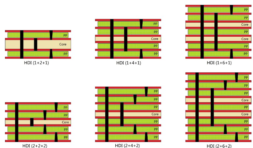
8-Layer Board (High-Speed, DDR, High-Speed Interfaces)
Classic 8-layer stackup:
Top – GND – Sig – PWR – GND – Sig – GND – Bottom
- Each signal layer is adjacent to a ground plane. The power plane is sandwiched between two ground planes, resulting in excellent power filtering and minimal crosstalk; this configuration is suitable for DDR, USB, and Ethernet applications.
High-speed board design rules of thumb: Keep signals close to reference planes; separate signal layers with ground planes; place power planes adjacent to ground planes; ensure a symmetrical stack-up.
IV. How to calculate key parameters
Use an impedance calculator (e.g., Si8000/Polar SI9000, or Altium’s built-in calculator).1. Input parameters for calculating 50Ω single-ended impedance
Inputs:1. Copper thickness T (convert oz to μm)
2. Dielectric thickness H (from signal to reference plane)
3. Dielectric constant Er (use the actual Er of the PP/Core from the PCB manufacturer, not the theoretical FR-4 value of 4.4)
4. Trace width W; trace spacing (if adjacent traces exist)
5. For outer layers, consider copper foil roughness; roughness reduces impedance.
• Larger H → Higher Z0
• Wider W → Lower Z0
• Higher Er → Lower Z0
Outer layer routing: Air (Er=1) on one side and dielectric (Er=4.2) on the other; thus, for the same W/H ratio, outer layer impedance is higher than inner layer impedance.
• Example: An inner layer 50Ω trace might be 4 mils wide, whereas an outer layer trace might need to be 5.5 mils wide to achieve 50Ω.
2. 100Ω differential impedance
• Additional parameter: Intra-pair spacing S.• Smaller S → Stronger coupling → Lower differential impedance.
• Note: Do not simply assume Zdiff = 2 × Zsingle.
• Example: For single-ended 50Ω, if S is very large (no coupling), differential impedance is 100Ω; as S decreases and coupling strengthens, differential impedance drops to 90Ω or 85Ω.
• Therefore: To achieve 100Ω differential impedance, single-ended impedance is often designed for 52–55Ω, then pulled back to 100Ω via coupling from trace spacing.
3. How to estimate dielectric thickness (stack-up thickness)
• Stack-up thickness = Sum of all Core thicknesses + Sum of all PP thicknesses + Top and bottom copper foil thicknesses. • PCB manufacturers provide specific PP (prepreg) types (e.g., 1080, 2116, 7628); the actual thickness varies after lamination.Key Point: The theoretical thickness defined in the software does not equal the actual post-lamination thickness. You must request a stack-up report from the manufacturer to obtain the actual dielectric thickness and Er (dielectric constant) values, then re-calculate impedance. Pitfall: Calculating impedance using theoretical PP values often results in significant deviations in the manufactured product.
4. Current-carrying capacity assessment (Power/High current)
• Factors include copper thickness, trace width, whether the copper layer is internal or external, and temperature rise.• Internal layers have poorer heat dissipation; for the same trace width, the current-carrying capacity is lower than that of external layers.
• For high currents, prioritize using internal power planes rather than relying on narrow traces.
5. Crosstalk assessment
Crosstalk is categorized into near-end crosstalk (NEXT) and far-end crosstalk (FEXT).Key influencing factors:
1. Dielectric thickness (h) between the signal trace and the reference plane; greater h results in greater crosstalk.
2. Spacing (S) between two traces; "3W rule": trace spacing ≥ 3 times the trace width.
3. Parallel coupling length of traces; longer parallel runs result in greater crosstalk.
4. Presence of a ground isolation layer between signal layers.
To minimize crosstalk: keep the dielectric between signal and ground as thin as possible; increase spacing between traces; avoid long parallel runs; route traces on different layers orthogonally (perpendicularly); and use ground layers to isolate signal layers.
6. Power-Ground coupling (Board-level capacitance)
• The smaller the dielectric thickness (h) between power and ground planes, the greater the parallel-plate capacitance.• C = ε0ErA/h
A smaller h results in higher capacitance. Therefore, using a thin dielectric between power and ground planes acts like a large built-in capacitor, suppressing power noise. For high-speed boards, select thin PP for the Power-GND dielectric layer.
7. Board warpage assessment
• Check for stack-up symmetry and copper area balance.• If one side has a large area of copper pour while the other is largely blank, warpage can occur even if the stack-up thickness is symmetrical, due to the asymmetry in copper area. 8. Impact of Vias on the Stack-up
• The stack-up configuration determines the via stub length. For high-speed signals, longer stubs result in more severe resonance.
• During stack-up planning, route high-speed signals on inner layers close to the surface layers to minimize stubs; use back-drilling when necessary.
V. Practical Circuit Design Workflow
Step 1: Clarify Project Requirements
1. Maximum signal rate: Low-speed (<100 MHz); Medium-speed (DDR3); High-speed (DDR4, USB3, PCIe, Ethernet)—high-speed signals require strict impedance control;2. Number of independent power rails required;
3. Estimated number of signal traces;
4. Board thickness requirements (common: 1.6 mm; others: 0.8 mm, 2.0 mm);
5. Cost constraints; requirement for impedance control;
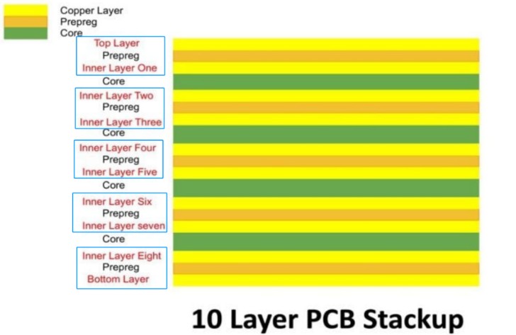
Step 2: Preliminary determination of layer count
• Low speed, few power rails: 4 layers;• DDR3, multiple power rails: 6 layers;
• DDR4/PCIe high-speed interfaces: 8 layers preferred;
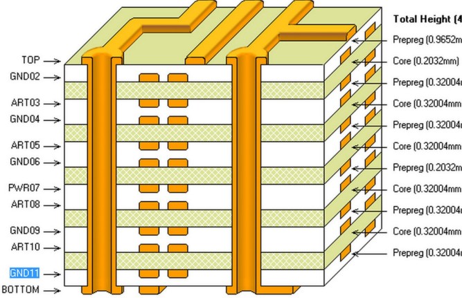
Step 3: Draft the layer stack-up, adhering to these rules:
1. Maintain symmetry as much as possible;2. Place every high-speed signal layer immediately adjacent to a solid GND plane;
3. Place power layers directly against GND layers;
4. Separate signal layers with ground planes whenever possible, avoiding direct signal-layer-to-signal-layer stacking;
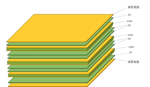
Step 4: Allocate dielectric thicknesses; contact the PCB manufacturer to obtain PP/Core specifications.
• Do not fabricate thickness values arbitrarily; request a list of available Core and PP materials from the PCB manufacturer, including post-lamination thicknesses and Dk values.Step 5: Impedance simulation and calculation.
• Input the manufacturer's actual Dk, copper thickness, and dielectric thickness to calculate trace widths and spacing for single-ended and differential signals.• Note that impedance requirements differ between outer and inner layers, necessitating different trace widths.
Step 6: Risk assessment.
1. Return path: Will the reference plane for high-speed signals be split?2. Crosstalk: Signal layer layout; is vertical routing between layers required?
3. Power coupling: Is the Power-GND dielectric thin enough?
4. Board warpage risk: Is the stack-up symmetrical, and is the copper distribution balanced?
5. Via stub length: Do high-speed signals require back-drilling?
6. Current-carrying capacity: Is the copper thickness of high-current power planes sufficient?
Step 7: Generate a complete stack-up document.
Document contents:• Layer sequence;
• Copper foil weight (oz);
• Dielectric materials for each layer (Core/PP model + post-lamination thickness);
• Dk/Df parameters;
• Target total board thickness;
• Impedance specifications: Single-ended 50Ω ±10%, Differential 100Ω ±10%;
The PCB manufacturer will provide an actual post-lamination stack-up report; verify this data and fine-tune impedance settings if necessary.