Analysis of PCB Warpage
Anyone working in hardware, PCB design, or SMT processing has likely encountered the pitfalls of PCB warpage.What might seem like minor board bending or warping can have disastrous consequences:
Component misalignment, cold solder joints, BGA voids, "tombstoning," misaligned screw holes, and cracking due to stress during final assembly—often leading to mass rework or the scrapping of entire batches.
Many mistakenly believe that PCB warpage is solely a manufacturing process issue.
In reality, 90% of warpage issues are predetermined during the schematic stack-up, layout, and material selection stages.
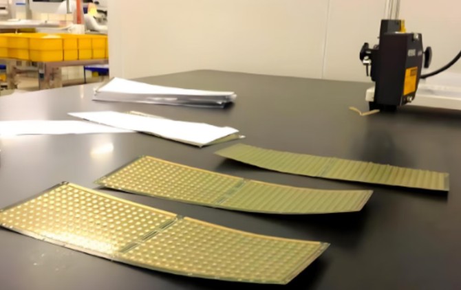
I. Why do PCBs warp? There are four fundamental causes.
The essence of PCB warping lies in uneven stress distribution across the board surface and inconsistent stress release.All forms of bending, twisting, and surface irregularities stem from these four categories of causes:
1. Mismatched thermal expansion (CTE differences)
The Coefficients of Thermal Expansion (CTE) differ among the core board, prepreg (PP), and copper foil. During lamination, high-temperature baking, and the thermal cycling of reflow soldering, these materials expand and contract at different rates. This generates permanent internal stress, ultimately manifesting as board warping.2. Deformation caused by thermal cycling
The resin and copper components of the board have different high-temperature characteristics. Repeated cycling between high and low temperatures leads to the accumulation of localized deformation, resulting in board bending or one-sided uplift.3. Mechanical stress during manufacturing (tension and uneven pressure)
Uneven lamination pressure, pulling forces during depaneling, compression from stacking during transport, uneven heating during SMT, and unbalanced fixture pressure can all cause mechanical deformation of the board.4. Material defects
Low glass transition temperature (Tg), uneven resin content, insufficient rigidity, and moisture absorption significantly reduce the board's resistance to deformation, making it highly susceptible to warping.
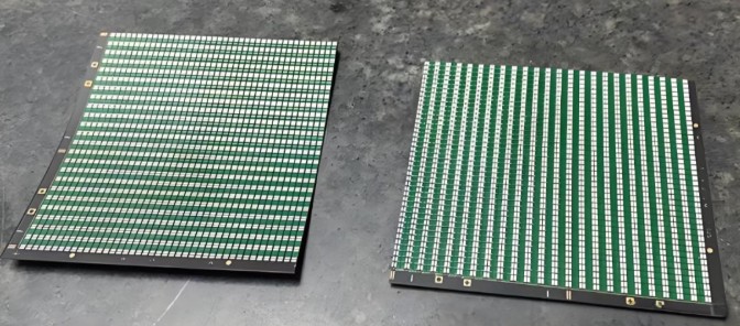
II. How to Measure PCB Warpage? Industry-Standard Methods (Including Strict Automotive Electronics Specifications)
✅ Standard Measurement Method: Flat Plate + Feeler GaugePlace the PCB naturally flat on a standard horizontal surface without applying any external pressure. Use a feeler gauge to measure the maximum clearance at the four corners and calculate the overall warpage.
Warpage Calculation Formula:
Warpage = Maximum Warpage Height ÷ Diagonal Length of the PCB
✅ Industry Acceptance Criteria
- General Consumer Electronics: Warpage ≤ 0.5% of diagonal length
- Automotive Electronics / Industrial Control / High-Reliability Products: Warpage ≤ 0.3% of diagonal length
Important Prerequisite: Before measurement, the PCB must undergo dehumidification baking and be allowed to stabilize at room temperature. This ensures data validity by eliminating interference from moisture or temperature.
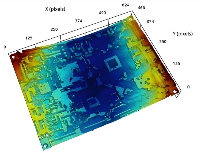
III. Improvements at the Source (I) Base Material & Auxiliary Material Optimization: Choosing the Right Materials Halves Warpage
1. Core Principles for Material Selection
- Low-CTE Matching: Prioritize core boards and prepregs (PP) with low coefficients of thermal expansion (CTE) to match the expansion/contraction characteristics of copper foil, thereby minimizing thermal deformation.
- High Rigidity & High-Temperature Resistance: For thick boards, high-layer-count boards (8 layers or more), and boards intended for high-temperature environments, select high-Tg, high-rigidity FR-4 materials to enhance resistance to deformation and stress.
- Material Uniformity for Asymmetric Boards: For special boards where symmetric stacking is impossible, standardize the model, thickness, and resin content of core boards and prepregs across the entire board to prevent uneven shrinkage caused by material disparities.
2. Balancing Copper Foil and Copper Thickness (Crucial)
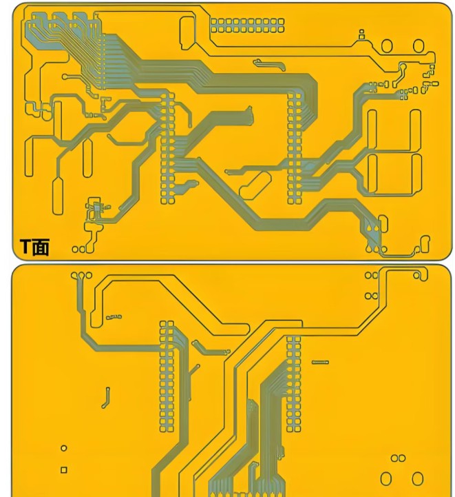
There is a vast difference in thermal expansion between copper and the board substrate; uneven copper distribution is the primary design-related cause of warpage.- Ensure copper area and thickness are as symmetrical as possible between the top and bottom layers; strictly prohibit solid copper pours on only one side or localized accumulations of thick copper.
- Replace solid copper areas (such as thick copper power planes or large copper pours) with hatched copper patterns and localized cutouts to effectively relieve thermal stress.
3. Precision Control of Prepreg (PP)
- Use the same batch and resin content of prepreg across a single PCB to eliminate variations in curing shrinkage.
- Use high-resin prepreg for high-precision and automotive boards to improve flatness; use low-resin prepreg for standard boards to reduce deformation caused by moisture absorption.
IV. Improvements at the Source (II) Layout & Stack-up Design: Eliminating Warpage at Zero Cost
Design optimization is the most cost-effective solution for warpage; it yields the most significant results without adding any cost.1. Stack-up Structure: Prioritize Absolute Symmetry
80% of warpage issues in multilayer boards stem from asymmetrical stack-ups.Stack-up design must ensure mirror symmetry between the top and bottom layers regarding core board thickness, number of prepreg sheets, copper thickness, routing density, and copper pour coverage.
Strictly prohibit: Large blank/unclad areas on one side or the concentration of dense pads/traces on only one side.
2. Copper Pour and Layout Optimization
- Convert large solid copper areas to a hatched (grid) pattern with an open area ratio of ≥30% to relieve thermal expansion and contraction stress.
- Incorporate stress-relief slots and process cutouts along the edges of large or long boards to release internal stresses generated during curing.
- Prohibit isolated large copper patches near BGAs and precision chips to prevent localized deformation or pulling forces that could lead to soldering defects.
3. Panelization and Structural Optimization
- Divide long or large boards into smaller units and reduce single-side spans to enhance board rigidity.
- Use a combination of connecting tabs and perforated break-away lines (stamp holes) for panelization instead of narrow, elongated connecting strips; this minimizes mechanical pulling and deformation during board depaneling.
- Increase the width of process margins for thin boards to significantly improve overall board rigidity.
4. Balanced Through-Hole Layout
Distribute via arrays—such as flow-through holes and thermal vias—evenly across large surface areas to ensure uniform heating and outgassing, prevent unilateral stress concentration, and suppress warping or deformation.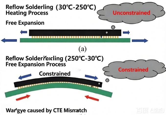
V. Process Improvement (III): Integrated Process Control for PCB Fabrication and SMT Assembly
1. Key Points for PCB Fabrication Process Improvement
- Lamination: Optimize temperature-pressure profiles to ensure uniform heating and cooling across the entire board; strictly control post-lamination cooling to prevent deformation caused by rapid temperature drops.
- Front-end Processes: Standardize parameters for material cutting, inner-layer processing, brown oxide treatment, and etching to minimize the accumulation of early-stage deformation.
- Surface Finish: Strictly control temperatures and conveyor speeds for ENIG (Electroless Nickel/Immersion Gold), HASL (Hot Air Solder Leveling), and OSP (Organic Solderability Preservative) processes to avoid deformation caused by prolonged exposure to high heat.
- Standardized Baking/Dehumidification: Implement uniform baking protocols prior to shipment and production input to eliminate deformation caused by moisture absorption.
2. Key Points for SMT Process Improvement
- Reflow Profile Optimization: Tailor heating, soaking, and cooling slopes based on the board's Tg (glass transition temperature) and thickness to prevent thermal warping caused by excessive temperature gradients.
- Fixture-Assisted Stabilization: Use dedicated carriers throughout the reflow process for thin boards, large boards, and high-precision BGA boards to constrain movement and suppress high-temperature deformation.
- Handling and Transfer Control: Prohibit stacking, compression, or bending; optimize the sequence of SMT placement and baking/pressing operations to avoid uneven localized stress.