A Must-Take Course on Vector Network Array (VNA) for All RF Engineers
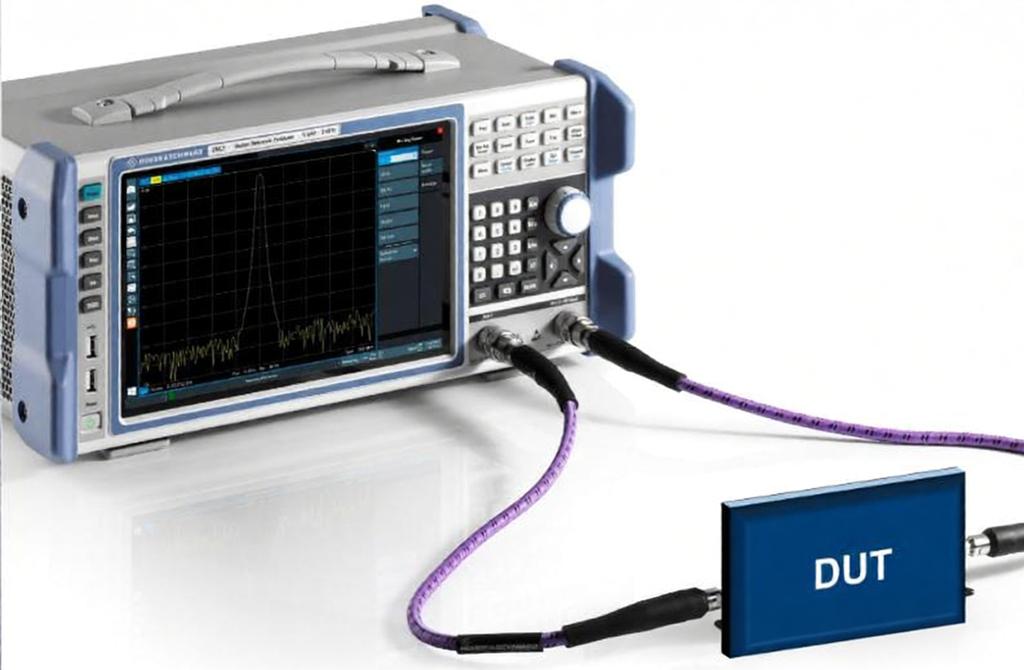
In the radio frequency (RF) industry, a network is a device with one or more interfaces (ports). Each port can do the following: conduct RF signals, absorb signals, or reflect signals back.

1. Single-port devices (one-port networks): Antennas and matched loads (dummy loads) belong to this category, with only one signal interface.
2. Two-port devices (two-port networks): Filters and power amplifiers are the most common, with one input and one output signal.
3. Three-port devices (three-port networks): Directional couplers and mixers have three signal interfaces.
The most commonly used devices in daily life are one-, two-, and three-port devices. Of course, there are also multi-port RF devices with even more interfaces.
Analyzing these RF devices (i.e., the RF networks mentioned earlier), the operating logic is simple: input an RF signal into any one of the ports, and then measure the signal power at two points: first, the signal power reflected back from the input port (reflected power); second, if the device has multiple ports, also measure the signal power leaking out/transmitting from each of the other ports.
In most conventional testing scenarios, only one port is used for signal input at a time; multiple inputs are not used simultaneously. Furthermore, the performance of these RF devices is entirely frequency-dependent, with different frequencies exhibiting different performance. Therefore, testing typically involves scanning an entire frequency range rather than measuring only a single frequency point. The instrument used for this type of testing is called a network analyzer.
The most common set of parameters describing the transmission and reflection of radio frequency (RF) signals is the S-parameter.
The letter S stands for Scattering, which simply measures the proportion of RF signals bouncing back and forth between various ports.
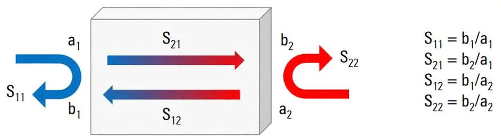
The naming convention for S-parameters is: a capital S followed by two subscripts. The first subscript indicates the port from which the signal exits, and the second subscript indicates the port from which the signal enters.
For example: if a signal enters from port 1 and exits from port 2, this transmission loss/gain is called S21; if a signal enters from port 1 and is reflected back from port 1, this reflection is called S11.
A radio frequency (RF) device with two interfaces (input and output) corresponds to four S-parameters: S11, S21, S12, and S22, each with the following meanings:
1. S11: The percentage of a signal input to port 1 that is reflected back from the device's input.
2. S21: The percentage of a signal input to port 1 that is normally transmitted to the output of port 2 (forward transmission).
3. S12: The percentage of a signal input to port 2 that is transmitted to the output of port 1 (reverse transmission).
4. S22: The percentage of a signal input to port 2 that is reflected back from the device's output.
All S-parameters are essentially power ratios, used to represent the proportion of signal reflection and transmission between the various ports.
Here are a few practical points about S-parameters:
1. S-parameters can be written as an N-order square matrix, where N is the number of ports on the device. Single-port, dual-port, and triple-port devices each have their own corresponding matrices.
2. S-parameters are not simply numerical values; they are complex numbers that contain both amplitude and phase information.
3. Reflection parameters like S11 and S22 are usually plotted on a dedicated Smith chart for visual reference.
4. The biggest advantage of S-parameters is that the S-parameters of individual devices can be cascaded and combined to directly calculate the overall performance of an entire RF link system without needing to rebuild and test the entire system from scratch.
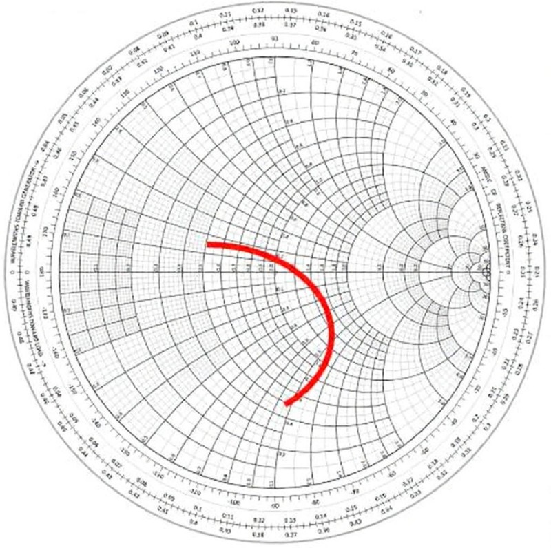
1. S11 and S22: These two reflection parameters represent the matching quality between the device's input and output, respectively. In the industry, they are generally quantified using return loss or VSWR (Standing Wave Ratio). These concepts will be discussed in detail later.
2. Transmission Parameters
- S21: Gain/loss in the forward transmission of the signal, i.e., whether the signal is amplified or attenuated as it travels from the input to the output;
- S12: Represents reverse isolation, measuring the degree of signal backflow, i.e., how much power leaks in the reverse direction.
For example, in a power amplifier: an ideal power amplifier should have amplification capability in the forward direction, resulting in a positive S21 value; simultaneously, in a perfect state, no power should flow back from the output to the input, meaning S12 should be close to 0.
VSWR and return loss are both used to reflect the transmission of RF power. One of the core requirements of RF circuits is to ensure efficient power transmission. To maximize RF power transmission, the impedances of the signal source and the downstream load (the device receiving the power) must be matched.
In this ideal state, all RF power output from the signal source is completely absorbed by the load, with no waste. Most circuits strive for this effect. The standard impedance in the RF industry is 50Ω; a few systems use 75Ω, with cable TV lines being a typical example.
What happens if the impedances of the signal source and the load are mismatched?
When impedance is mismatched, a portion of the forward signal power sent by the signal source will be bounced back by the load and flow back to the signal source. This bounced-back power is called reflected power, or reverse power; these two terms will be used interchangeably in the following explanation. Reflected power is generally considered undesirable; almost no scenario would want a signal to travel back from the load to the signal source.
Previously, when discussing impedance, we only used pure resistance as an example. However, in actual circuits, the impedance of any load is a complex impedance, divided into two parts: a real resistive component and an imaginary reactance component (characteristics of capacitance and inductance).
To achieve perfect impedance matching, the complex impedance of the load must match the conjugate complex impedance of the source—simply put, the resistance values must be the same, while the signs of the reactance must be reversed. Before we go any further, let's briefly review some basic impedance concepts.
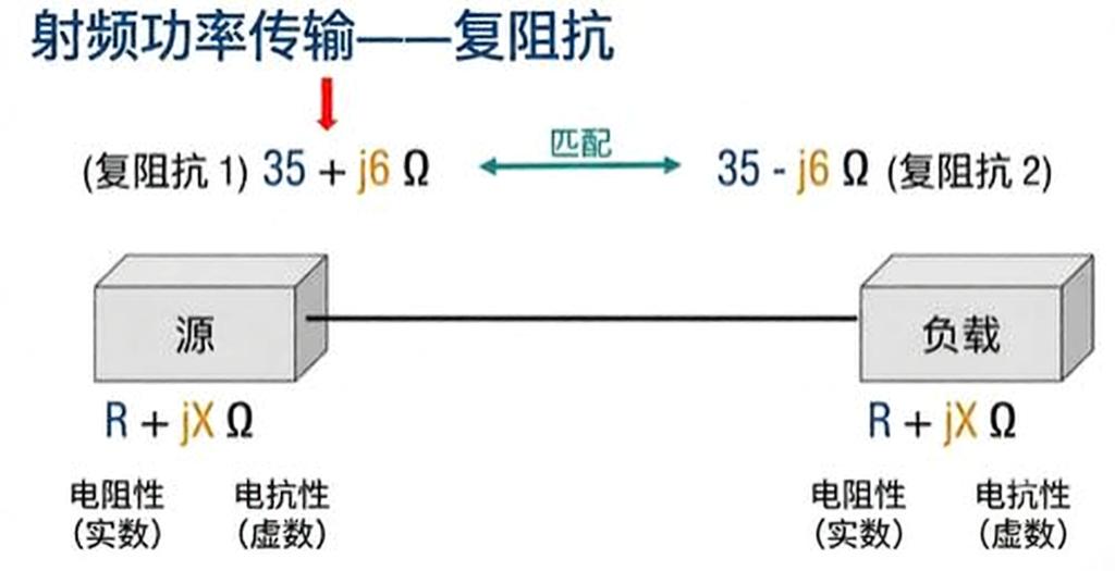
Remember that impedance Z is a complex number, consisting of two parts:
1. Resistance R: Its value does not change with frequency;
2. Reactance X: It changes with frequency.
Reactance is further divided into two types: capacitive reactance and inductive reactance, which are characteristics of capacitors and inductors, respectively. Complex impedance has both magnitude and phase angle.
Key point: Because of the presence of reactance, the overall impedance of a device changes with frequency; impedance varies at different frequencies.
How much does impedance change with frequency? It depends entirely on the load device itself. For example, an RF dummy load is essentially a purely resistive structure, specifically designed to maintain stable impedance over a wide frequency range.
In contrast, the impedance of most antennas fluctuates significantly with frequency. This is why each antenna is labeled with its specific operating frequency band and can only be used within that band. Another point to note is that in actual use, antenna impedance is also affected by the installation environment, such as the distance between the antenna and a grounding metal plate or surrounding metal objects, all of which will change its impedance.
If we use a near-purely resistive dummy load as the back-end load, even if the frequency is adjusted from 100MHz to 200MHz, 500MHz, or even 1GHz, the reflected signal power will remain consistently low and show little change.
However, if we use an antenna as the load, the reflected power will vary greatly with frequency. The characteristics of most RF devices on the market fall somewhere between these two extremes: one where impedance hardly changes with frequency (dummy load), and another where impedance fluctuates significantly and irregularly with frequency (antenna).
Therefore, we definitely need a metric to measure the reflected power, and it's usually compared to the transmitted forward power. There are two industry standards for describing this ratio: return loss and Voltage Standing Wave Ratio (VSWR). Let's start with return loss.
Return loss, simply put, is the dB difference between the forward transmitted power and the reflected power.
Simply remember: Forward power dB - Reflected power dB = Return loss.
For example: If the transmitted power is 50dBm and the reflected power is 10dBm, then the return loss is 40dB. A higher return loss value means less signal is reflected back, so we always want a higher return loss in circuit design. Moreover, return loss is always a positive number because the reflected power can never be greater than the transmitted power. Even in extreme cases where the load reflects the entire signal back, some power will be lost during the signal's round-trip transmission, so the reflected power will still be less than the forward power.
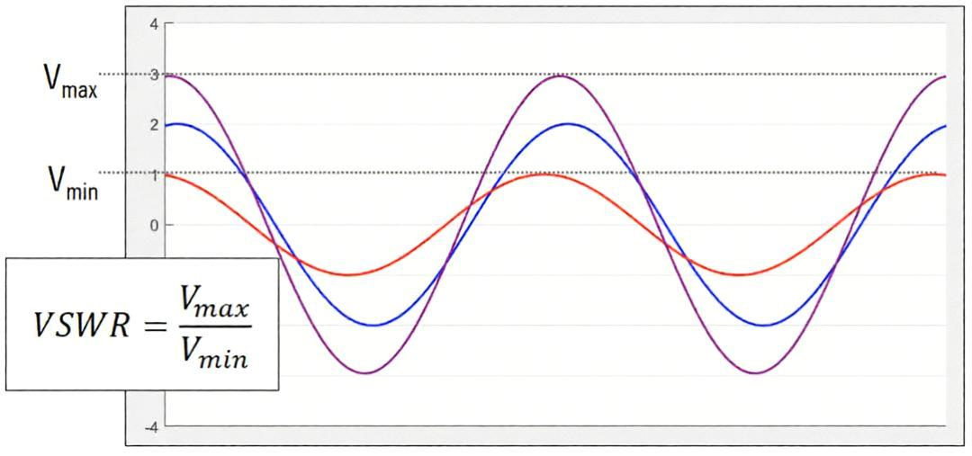
Another metric used to compare the magnitude of reflected and forward signals is VSWR, or Voltage Standing Wave Ratio. In the graph, the blue curve represents the voltage waveform of the forward signal, the red curve represents the reflected voltage waveform, and the purple curve represents the total voltage actually present on the transmission line after the two waveforms are superimposed.
The voltage amplitudes of the forward and reflected waves are constant, but the total voltage after their superposition will fluctuate. This fluctuating waveform is called a standing wave.
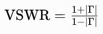
VSWR is calculated simply as: Maximum voltage on the standing wave ÷ Minimum voltage.
In the example in the text, the peak value is 3 and the valley value is 1, so the VSWR is 3:1. It's commonly said that VSWR = 3.
Two additional points:
1. Many amateurs simply abbreviate it as SWR, omitting the leading V;
2. The current standing wave ratio and the voltage standing wave ratio are exactly the same, but no one uses the term "current standing wave ratio CSWR".
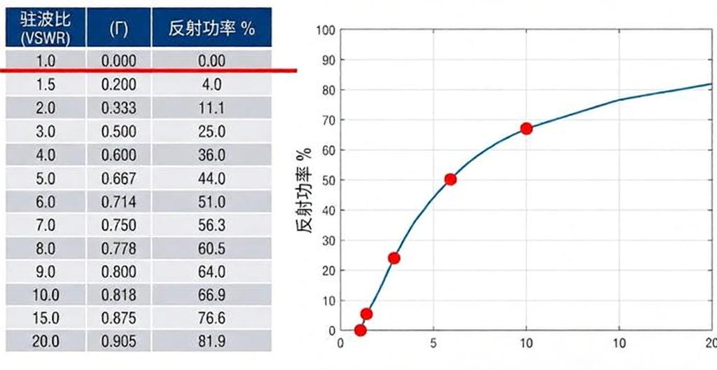
After understanding how VSWR is calculated, let's look at what a larger VSWR value means:
1. When the source and load impedances are perfectly matched, VSWR=1, there is no signal reflection, and all transmitted power is absorbed by the load.
2. VSWR=1.5: Only 4% of the power is reflected back, with very low loss.
3. VSWR=3: A quarter of the power bounces back to the signal source, which is barely acceptable in most scenarios.
4. If VSWR continues to increase, the reflected power will surge:
- VSWR=6: Only half of the power is absorbed by the load, and the other half bounces back along the same path;
- VSWR=10: Two-thirds of the transmitted power will be reflected back, resulting in significant waste.
There are two extreme special cases of VSWR that need to be discussed separately:
The first is a short circuit: the load impedance is equal to 0, and the reflection coefficient Γ = -1;
The second is an open circuit: the load impedance is infinite, and the reflection coefficient Γ = 1.
Regardless of whether Γ = 1 or Γ = -1 is substituted into the VSWR calculation formula, the calculated VSWR will always be infinite, meaning that 100% of the transmitted power is reflected back to the signal source.
Needless to say, total power reflection is generally undesirable and can severely damage transmitting equipment.
Leaving aside the extreme cases of open circuits and short circuits, how should we handle signal reflection in everyday situations?
The most common way to reduce reflected power is to add a tuning matching network between the signal source and the load. This matching network consists of reactive components such as capacitors and inductors. By adding extra impedance, it transforms the originally mismatched load impedance into an impedance that matches the source.
For example, if our goal is to transform the complex load impedance into a pure resistance of 50Ω to match a standard 50Ω signal source, by using appropriate capacitance and inductance values in the matching network, we can adjust the overall equivalent load impedance to perfectly match the source impedance, significantly reducing signal reflection.
Another method to reduce the impact of reflected power is to directly reduce the transmit power. This mechanism is called power backoff and is mainly used in high-power equipment, such as broadband power amplifiers. The core function of power backoff is to protect the signal source: excessive reflected power will degrade equipment performance and, in severe cases, permanently burn out hardware.
For example: Suppose the maximum safe reflected power allowed by the device is 40W.
1. With good impedance matching and VSWR=1.5, a 100W forward transmission will only reflect 4W back, within the safe range.
2. If the impedance deteriorates, the VSWR rises to 6. The same 100W transmission power will produce 50W of reflected power, exceeding the safe limit.
3. At this point, power backoff is initiated, reducing the transmission power to 80W, and the reflected power will fall back below the safe threshold.
Measurement accuracy and repeatability are always critical, and it's certain that Vector Network Analyzer (VNA) measurements are among the most error-critical test scenarios in the RF field.
We typically categorize measurement errors into three main types: drift error, random error, and systematic error. Sometimes, random error and drift error are grouped together as random errors.
Regardless of the type of error, all errors will cause deviations in the amplitude and phase of the measured signal; that is, the error itself is a vector. Below, we briefly introduce these three types of errors.
Drift error arises from environmental changes after calibration, with the majority of drift stemming from temperature fluctuations. Therefore, the primary methods to reduce drift error are: firstly, to stably control the test environment temperature; and secondly, to allow the instrument sufficient warm-up time. Another approach is to recalibrate after environmental changes, which can also offset drift error. However, even with all these measures, drift error can only be reduced significantly, not completely eliminated.
Drift error is mostly caused by the environment, while random error primarily originates from the entire test setup. This includes instrument noise, test operations and parameter settings, and even differences in cable and connector contact during each installation, all contributing to random error. It's called random error because it changes irregularly over time, resulting in different and unpredictable measurement results each time. Using high-end equipment and standardizing test operations can effectively reduce random error. However, like drift error, it can only be reduced, not completely eliminated.
Systematic error differs from drift and random error in that it is reproducible, predictable, and does not change over time. The root cause lies in the fact that systematic errors primarily originate from within the vector network analyzer and from various non-ideal components in the test link.
Typical sources of systematic errors include:
1. Defects in the instrument's own components, such as directional couplers not achieving ideal isolation or directivity;
2. Inherent losses in the test cables;
3. Impedance mismatches at various points in the link.
The biggest advantage of systematic errors is that they can be almost entirely eliminated through calibration.
Calibration is a set of procedures for eliminating systematic errors in measurement results. Before calibration, you must select a corresponding calibration scheme based on your test link structure and desired test accuracy. Various calibration types will be introduced later.
Then, connect the dedicated device—the calibration component—to the input port of the device under test (DUT) in the test link. Start the instrument's calibration program, and the instrument will collect response data from the corresponding ports. Many calibration schemes require repeatedly replacing and plugging in different calibration components, or sequentially connecting them to different ports. The entire set of collected calibration data will be saved. When subsequently testing the DUT, the instrument will use this data to correct the measured values and offset systematic errors.
It is crucial to distinguish between test calibration and instrument metrological calibration, as they are entirely different:
1. Test Calibration: Its purpose is to eliminate systematic errors in VNA testing. This is performed by the test personnel and is frequently used, typically before each test or critical test. The instrument interface displays a "Cal" icon, indicating a valid test calibration is in place.
2. Instrument Metrological Calibration: This verifies whether the instrument's specifications meet factory specifications. For example, when setting the output power to -10dBm, does the instrument actually output -10dBm?
This calibration is not performed by the user but by a third-party metrology organization. It has a fixed cycle, usually every few years. The instrument's metrological calibration is valid only if the metrology sticker on the instrument body is intact and has been calibrated within the last few years.
Another key concept in calibration is the calibration reference plane, which is the reference position where calibration takes effect. In most scenarios, the device under test (DUT) is not directly plugged into the vector network analyzer port; a cable or even an attenuator connects the DUT and the instrument port. By setting the calibration reference plane at the connection point of the device under test (DUT), the influence of all cables and components between the DUT and the instrument port will be canceled out by calibration.
Calibration requires calibration kits, which are typically sold as sets. These kits include loads, couplers, and other components whose amplitude and phase responses are calibrated with extremely high precision, meaning we know exactly what values we should theoretically obtain when measuring them.
Standard response data is usually stored in the calibration kit definition file, which is generally pre-installed on the instrument or can be imported via USB. By testing the calibration kit and comparing the results with its known standard values, we can calculate the amplitude and phase errors introduced by the VNA and the entire test link.
The four most commonly used calibration kits are through-hole, open-circuit, short-circuit, and matched load (sometimes simply called load). Their names give a general idea of their electrical characteristics, but one crucial point is that even these basic calibration kits are not ideal devices; non-ideal characteristics become more pronounced under wideband testing.
For example, at frequencies exceeding 100MHz, open-circuit components generate parasitic capacitance. This is why the parameter definitions of the corresponding calibration kit must be entered into the VNA.
The parasitic parameters of open-circuit components vary between manufacturers and models; you cannot use just any open-circuit component for calibration, otherwise the measurement accuracy will be very poor.
Calibration kits mainly come in two forms: standalone components and calibration T-type heads that integrate four standard components: through, open, short, and matched load. When using these types of calibration kits, manual plugging and unplugging is required during the calibration process.
Automatic calibration modules (Autocal) are becoming increasingly common. They also integrate through, open, short, and matched load components, but can automatically switch between different standard components during calibration, controlled entirely by the VNA via USB.
Automatic calibration modules come with parameter files for their internal standard components, which the instrument can directly read and call.
Automated calibration significantly reduces manual operation, offering clear advantages:
1. It is far faster than manual calibration; the efficiency difference becomes more pronounced with the number of ports.
2. It reduces human error, such as connecting the wrong calibration component or selecting the wrong kit parameter file.
3. Relying on electronic switches, it eliminates the need for repeated plugging and unplugging, greatly reducing wear on calibration component connectors.
The calibration scheme essentially specifies which standard components (through, open, short, matched load) are used in the calibration process, and at which step and on which port the corresponding standard component is connected.
We need to select a suitable calibration scheme based on several conditions:
2. Is only unidirectional transmission measured between dual ports, or both directions?
3. How high is the required measurement accuracy, and how much calibration time can be allocated?
4. What available calibration components are available?
The following will briefly introduce some of the most commonly used calibration methods in single-port and dual-port testing: reflection normalization, complete single-port calibration, transmission normalization, single-path dual-port calibration, and two complete dual-port calibration schemes.
Let's start with single-port calibration, which is only used for reflection parameter testing. There are two main types of single-port calibration: the first is complete single-port calibration, which takes the longest but offers the highest measurement accuracy. It's slow because it requires connecting three calibration components sequentially to the calibration reference plane: an open-circuit calibration, a short-circuit calibration, and a matched load calibration. The other type is normalization calibration, which is faster but less accurate. The core reason is that it only requires connecting a single standard component, using either an open circuit or a short circuit.
Two-port calibration is primarily used for transmission parameter testing. Like single-port calibration, it falls into two categories: normalization calibration, which is fast but has lower accuracy, and complete calibration, which is time-consuming but more accurate.
Transmission normalization calibration is simple to operate, requiring only a single standard component (a pass-through) and can be performed unidirectionally or bidirectionally.
Between normalization and complete two-port calibration is single-path two-port calibration: it performs a complete single-port open-circuit-short-load calibration at one end, combined with transmission normalization. However, it only optimizes the test accuracy in a single transmission direction.
If both ports undergo complete single-port calibration, it constitutes complete two-port calibration, which mainly has two types:
1. TOSM (Pass-Through-Open-Short-Load) Calibration
2. UOSM (Unknown Pass-Through-Open-Short-Load) Calibration
These two types of complete two-port calibration are described in detail below.
Pass-Through-Short-Open-Load Calibration (TOSM) is the most widely used calibration scheme in two-port testing. After completing TOSM calibration, the reflection parameters of both ports and the bidirectional transmission parameters between them will be corrected for errors, allowing measurement of all S-parameters.
Its only drawback is its cumbersome and time-consuming operation, requiring a total of 8 scans: each port is sequentially connected to three standard components—open circuit, short circuit, and matched load—for single-port calibration, then a through-hole is connected between the two ports, and scans are performed separately in both transmission directions. A major advantage of the Autocal automatic calibration module is its ability to automatically complete the entire TOSM process within seconds, eliminating the need for manual repeated insertion and removal of calibration components.
Unknown Through-Open-Short-Load Calibration (UOSM) uses an "unknown through-hole" to replace the standard known through-hole; a general-purpose RF coupler can typically serve as the unknown through-hole. This unknown through-hole only needs to meet the requirement of consistent bidirectional electrical characteristics. This calibration is ideal for scenarios where the connectors at both ends of the device under test (DUT) have different specifications, such as one end being an SMA connector and the other an N-type connector.
Finally, there is a complementary calibration step: isolation testing, which is generally used in conjunction with through-hole calibration. Straight-through calibration acquires the useful signals transmitted normally between ports via cables and devices; while isolation testing measures the signal leakage and crosstalk within the instrument ports.
Isolation testing does not require dedicated calibration components; standard operation involves connecting a 50Ω matched load to both test ports. Modern vector network analyzers have excellent internal isolation, making measurement errors due to crosstalk negligible.
In summary: RF devices are classified as single, dual, and triple-port, and their signal reflection and transmission characteristics are commonly characterized by S-parameters. Impedance matching quality can be quantified using VSWR and return loss. Impedance mismatch generates reflected power, which can harm equipment performance. Impedance can be optimized through matching networks, or power backoff can be used to protect high-power devices. VNA measurements exhibit three types of errors: drift, random, and systematic. Only systematic errors can be eliminated through testing and calibration, requiring regular third-party instrument calibration. Calibration relies on various standard components, including manual and automatic calibration, and offers multiple single-port and dual-port calibration schemes to suit different testing accuracies and scenarios. Isolation testing can identify port crosstalk errors.