PCB Micro-via Back-drilling Technology Research
As product cycles in the telecommunications and electronics industries accelerate, PCBs—often referred to as the "mother of electronic products"—demand increasingly stringent quality standards for micro-via processing. Back-drilling, a critical process for removing unnecessary copper from through-holes and controlling stub length, directly impacts high-speed signal integrity. Since back-drilling typically occurs after through-hole metallization, the processing conditions differ fundamentally from standard through-hole drilling; consequently, issues such as hole clogging, positioning accuracy, and stub length control have become core challenges hindering the advancement of micro-via back-drilling technology. While existing research has largely focused on applied aspects—such as process optimization, machining parameters, processing methods, and micro-drill geometry—a systematic understanding of the underlying mechanisms remains insufficient.The Unique Nature and Key Challenges of Back-Drilling
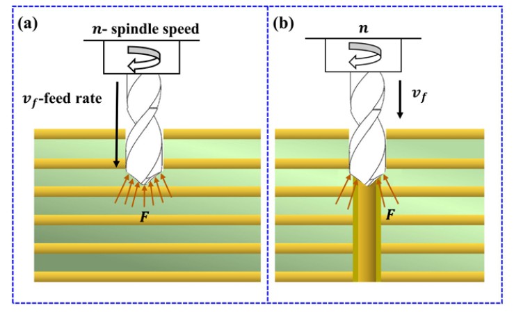
Standard through-hole drilling involves penetrating the entire PCB, subjecting the micro-drill's entire cutting edge to material reaction forces and resulting in a relatively continuous loading state. In contrast, back-drilling targets a hole that has already undergone metallization and features an internal copper plating layer; here, the drill tip does not participate in effective cutting, and only the side cutting edges contact the material, creating a localized loading condition. This asymmetric loading characteristic makes the back-drilling process highly sensitive to hole positioning accuracy and tool rigidity. Furthermore, back-drilling requires re-clamping and re-positioning the PCB; even minute positional deviations can cause uneven forces on the drill bit, leading to "drill walking," which may result in hole curvature or even drill breakage. Therefore, the diameter of a back-drilling micro-drill is typically at least 0.15 mm larger than the through-hole diameter to ensure adequate positioning tolerance.
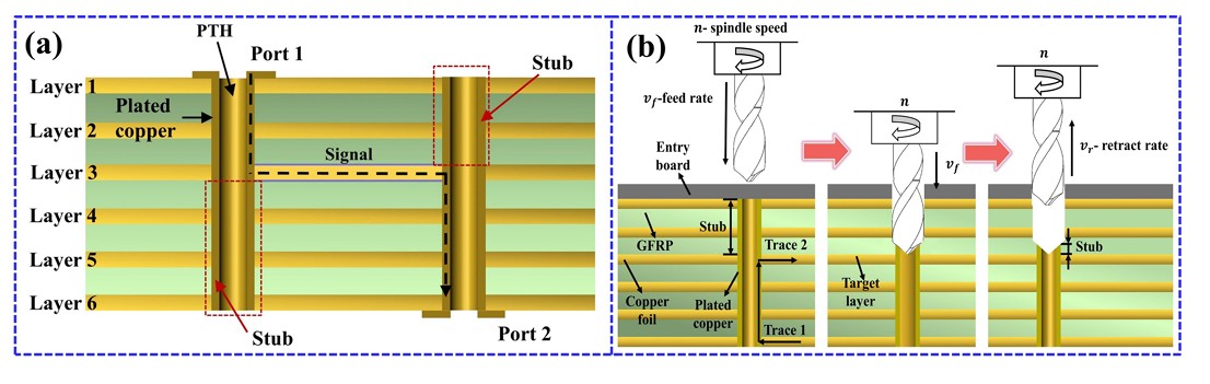
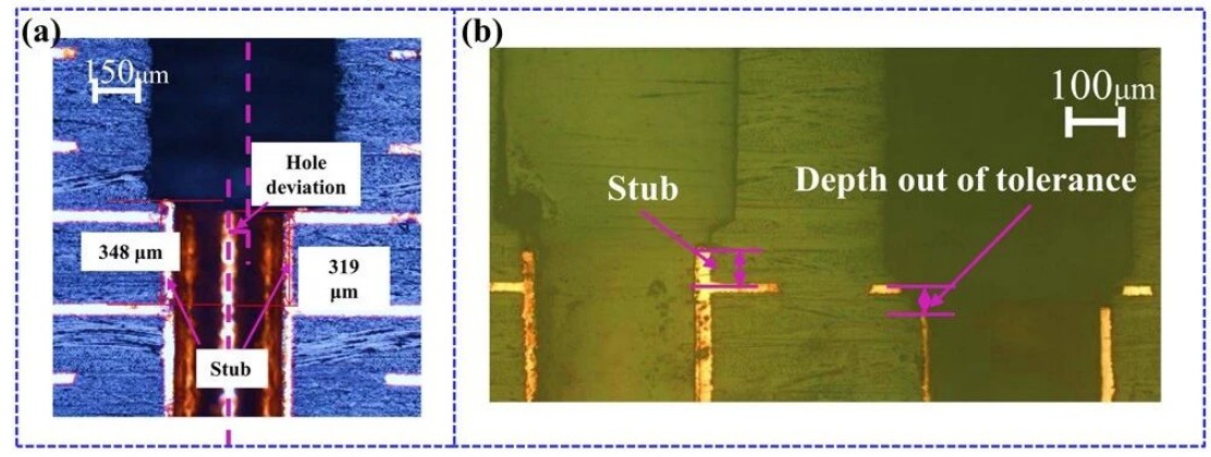
Back-drilling microvias in high-speed boards presents stringent requirements regarding microvia quality, positional accuracy, and stub length due to the materials' difficult machinability, small hole diameters, and significant depths. Specifically, the process faces three major challenges. First, drilling heat causes the resin in high-speed boards to agglomerate into polymers that adhere to the micro-drill bit, leading to issues such as hole-wall debris, filamentation (stringing), and hole clogging; clogging is the most frequent problem, as chips fail to evacuate promptly and block the microvia, severely compromising signal transmission quality. Second, as hole diameters shrink, the tolerance for positional deviation tightens; off-center back-drilling results in excessive residual stubs, adversely affecting signal transmission. Third, the increased aspect ratio of microvias makes precise control of back-drilling depth difficult; excessive depth removes the functional via copper along with the stub, rendering the microvia incapable of signal transmission or even causing the entire board to be scrapped.
Mechanisms and Process Strategies for Addressing Hole Clogging
Fundamentally, hole clogging occurs when the rate of chip generation exceeds the rate of chip evacuation. During back-drilling, chips consist of a mixture of dissimilar materials—resin, glass fiber, and plated copper. The plated copper is ductile and resistant to fracturing, and the presence of existing via plating further restricts the space available for chip evacuation; these combined factors make chip removal particularly difficult. The thickness of the via copper is a critical factor; excessive plating thickness directly reduces the available space for chip evacuation. Liu Xiaohua and colleagues addressed this by increasing evacuation space—specifically by reducing the via copper plating thickness and implementing a post-back-drilling treatment—thereby completely eliminating microvia back-drilling clogs; however, the applicability of this method is limited by customer specifications regarding copper plating thickness.
Regarding tool optimization, tungsten carbide (WC) has become the primary material for back-drilling micro-drills due to its excellent wear resistance, high rigidity, extremely low thermal expansion coefficient, and high fracture strength. The A129BD back-drilling tool features a design characterized by a short flute length, a small helix angle, and a thin web thickness; testing has shown that it significantly mitigates issues related to hole clogging and misalignment during back-drilling. The drill point angle also plays a significant role in cutting and chip evacuation performance; compared to standard 165° drill bits, specialized back-drilling bits with a 130° point angle drastically reduce clogging rates, effectively resolving the problem.
Factors Influencing and Controlling Back-Drilling Positioning Accuracy
Reducing the back-drilling hole diameter necessitates a corresponding reduction in drill bit diameter, which compromises the bit's flexural strength and concentricity. This makes the bit prone to slipping upon entry, leading to random positional deviations and reduced positioning accuracy. Furthermore, wear resulting from continuous drilling operations can degrade cutting precision. The use of entry sheets (cover boards) has proven effective in enhancing positioning accuracy; specifically, lubricating resin within aluminum-resin composite sheets adheres to the micro-drill, providing lubrication and reducing wear. Additionally, combining a high-rigidity drill bit with a low feed rate helps suppress drill bit oscillation. Relevant experiments utilized a laminate of aluminum and phenolic resin sheets as the entry sheet, thereby simultaneously addressing the requirements for positioning and lubrication. Regarding the influence of machining parameters on hole position deviation, researchers employed a combination of BP neural networks and orthogonal experiments to determine the optimal parameters for a 0.35 mm micro-drill: a spindle speed of 150 krpm, a limit of 1,800 holes, and a feed rate of 115 ipm; an effective neural network model was also established to guide actual production. It has been further observed that positioning accuracy improves with increases in spindle speed, retraction speed, and drill bit diameter, while it decreases with increases in feed rate, the number of drilled holes, and entry board thickness. Nevertheless, research specifically addressing back-drilling positioning accuracy remains relatively limited. Variations in positioning accuracy alter the contact conditions between the back-drilling cutting edge and the material, thereby affecting the axial drilling force—a relationship that warrants further in-depth mechanical analysis.
Precise Control of Residual Stub Length
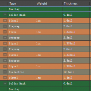
The length of the residual stub resulting from back-drilling is closely linked to high-frequency, high-speed signal integrity. As the layer count and thickness of high-speed PCBs increase, inter-layer thickness non-uniformity arises; variations in board thickness have been identified as the primary factor affecting stub control. By employing a novel lamination layup—combining silicone pads, epoxy backing boards, and aluminum sheets—the thickness differential between copper-populated and copper-free areas can be limited to within 0.053 mm. This approach enhances board thickness uniformity and minimizes errors in stub length caused by thickness variations.
Review of Current Research and Directions for Theoretical Advancement
Overall, existing research on back-drilling technology has yielded substantial engineering-level achievements in areas such as suppressing hole plugging, improving positioning accuracy, and controlling stub length. These efforts—primarily focused on optimizing process parameters, improving tool geometry, and innovating machining methods—have provided effective solutions to practical challenges in micro-via back-drilling. However, the back-drilling process involves a complex interplay of factors, including asymmetric localized cutting, mixed-chip flow from heterogeneous materials, constraints imposed by metallized hole walls, and coupled errors from secondary positioning. There remains a lack of in-depth theoretical analysis regarding the underlying mechanical behavior and material removal mechanisms. Future research should establish systematic models—incorporating perspectives such as cutting mechanics, the evolution of contact states, and chip evacuation dynamics—to elucidate the fundamental principles of back-drilling. Such insights will provide a more reliable theoretical foundation for the precision control of micro-via back-drilling processes in high-speed circuit boards.