From schematics to reliable products: 5 mistakes hardware engineers should never make
The cruelest thing about hardware development is that if you do a hundred things right, May nobody remembers; but if you make one mistake, everyone may remembers.From schematics to mass production, some mistakes, once made, can lead to anything from burnt-out boards to recalls. I'll break down the five worst mistakes you can make, each with a real-life, painful example.
Mistake 1: Disregarding the Laws of Physics, Forcibly Downgrading Layers
"Can a four-layer board be converted to a single-layer board?"
An engineer with ten years of experience bluntly stated: "Converting a four-layer board to a single-layer board? This isn't design; it's magic."
Finally, someone asked the crucial question: "How many pins?" The answer was: "Approximately 400 pins." The engineer paused for a moment and said: "It can be done, but half the functionality will be cut, the processor will need to be downgraded, and high-speed interfaces cannot be used."
Why was this mistake fatal?
A four-layer board has a complete ground plane and power plane, a reference plane for signals, and a clear return path. A single-layer board—has nothing. High-speed signals lack a reference plane, impedance cannot be controlled, and EMI directly exceeds limits.
Ultimately, the company abandoned the idea of a single-layer board. The engineers proposed a compromise: reduce the four-layer board to two layers, lowering costs by 30%, with manageable performance loss. Costs were reduced, but product launch was delayed by two months.
Remember: Not all boards can be downgraded. Hardware engineers must adhere to professional judgment and fully assess design feasibility. Some physical laws cannot be circumvented.
Mistake Two: Chaotic Version Control, Sending the Wrong Files
This case is even more outrageous.
A development team was rushing a project and, to shorten the timeline, completed the PCB and SMT assembly on a one-stop PCB platform. The factory received the boards and immediately assembled them, only to find that none of the functions worked during power-on testing.
After much investigation, it was discovered that capacitors C1 and C2 on the circuit board were short-circuited between power and ground. Initially, it was assumed the board manufacturer had made a mistake, but further investigation revealed that the engineer had sent the wrong PCB file.
Many versions were revised, and even the engineer himself got confused.
Fortunately, this only involved 100 boards. If it were thousands, the consequences would range from rework to complete board scrap.
Why is this mistake so basic?
Because it has nothing to do with technical ability; it's purely a matter of engineering habits. A single oversight in version control can render the entire team's efforts futile.
How to fix it?
Schematic, PCB, and BOM must strictly match version.
Check each board layer by layer with Gerber viewer before each submission.
Have a second person review the board before it's shipped.
Don't trust "I remember it's this version."
Mistake 3: Focusing only on "usability," not "ease of installation."
The placement of a single capacitor reveals the entire team's design thinking.
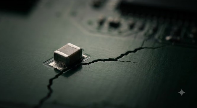
Next to the PCI slot of a network card, the capacitor pad is right next to the gold fingers. During normal installation, the PCI slot will be under stress towards the motherboard, and that capacitor is right in the stress zone—essentially putting the capacitor on a hot plate.
A novice assembler might easily break the capacitor leads or detach the pad during assembly.
Let's do the math: 100,000 units shipped annually, a 1% return rate, and a repair cost of 30 yuan per unit—300,000 yuan wasted annually. And that doesn't even include the damage to brand reputation.
Why is this mistake so common?
When hardware engineers design boards, they often think about "electrical connectivity." "How easy is it for workers to assemble?" or "Will the assembler be abusive?"—these are not considered.
However, problems with DFA (Design for Assemblability) and DFM (Design for Manufacturability) are far more costly than electrical errors. Electrical errors can be detected during debugging, but assembly problems are often discovered on the production line, which is too late.
What to do?
Consider "space redundancy" and "stress dispersion" during the layout phase.
After design completion, involve structural engineers and production line workers in the review.
Perform simulated insertion and removal tests using real components.
Establish a review checklist: Is the spacing up to standard? Is it in a stress zone? Does it affect testing?
Mistake Four: Not calculating impedance and blaming the PCB manufacturer
"Don't you need to calculate impedance for high-speed lines? Just hand it over to the PCB manufacturer, right?"
In June 2026, a newcomer posed this question in the industry, almost causing veterans to have a heart attack.
A senior layout engineer retorted directly: "If you don't calculate impedance, the PCB manufacturer won't be able to adjust it after you finish drawing it, and they'll send it back for you to redraw?"
A common misconception among beginners is that PCB manufacturers have a universal formula and that telling them the trace width will calculate the impedance. But the reality is— Scenario 1: The PCB manufacturer reports that the calculated DDR line impedance is 55Ω, not 50Ω.
Scenario 2: The PCB manufacturer reports that for this differential impedance, the trace spacing must be reduced to 3mil, but the manufacturer's process doesn't support this.
Scenario 3: The PCB manufacturer reports that your layer stack-up simply cannot achieve the required impedance.
The result? BGA fanout needs to be modified, the entire board routing needs to be redesigned, and timing constraints are completely messed up. A week is wasted on an impedance calculation that could be solved in five minutes.
What's the correct approach?
From the project's inception, "share the secret" with the PCB manufacturer—finalize the layer stack-up template during the project initiation phase: what board material to use, copper thickness, and dielectric thickness distribution. Complete multiple projects to build your own standard layer stack-up library.
Remember: High-speed lines not only need impedance calculations, but they need to be calculated before you even start writing.
Mistake Five: Ignoring Power Integrity and Ground Bounce
This is the most insidious and fatal mistake.
Case One: A Hole in the Power Layer
On a 12-layer server motherboard, the power layer below the main chip was squeezed by structural components, necessitating a large hole in the power layer to make way. During debugging, the CPU core voltage ripple measured 45mV, far exceeding the 25mV upper limit specified in the datasheet.
Replacing capacitors and adjusting feedback parameters took almost two weeks, but the ripple wouldn't come down. Finally, it was discovered that a 12mm x 8mm hole had been made in the Vcc layer directly below the CPU by a heatsink screw stand.
Temporarily patching it with a few copper foil pieces using jumper wires immediately reduced the ripple to 22mV.
Why does making a hole have such a significant impact?
High-frequency current doesn't follow the path of least resistance, but rather the path of least inductance. With a hole directly under the chip, the current has to detour, increasing the loop area, causing the PDN impedance to spike, and naturally, the ripple to increase.
Case 2: Ground Bounce Burns Out 5000 Circuit Boards
A smart lock manufacturer produced 5000 units, and 15% of the circuit boards inexplicably burned out their main control chips during high-temperature aging. Several hundred boards tested in the lab showed no problems.
The problem was ultimately discovered to be ground bounce noise—peak voltage reaching 2.3V! In a 3.3V system, the ground potential jumped directly to two-thirds of the power supply voltage, subjecting the chip pins to reverse voltage, eventually causing breakdown.
A recall and compensation for customers cost over 400,000 yuan.
Where did the ground bounce come from?
When multiple I/O ports toggle simultaneously, transient currents are generated. The ground line has parasitic inductance, U=L×di/dt, causing the ground potential to "boom."
How to address this?
A complete ground plane—lowest cost, best effect; avoid unnecessary slots and holes.
Decoupling capacitors should be placed as close as possible to power pins; vias should be as short and thick as possible.
Signal lines must have a complete ground plane underneath; high-speed lines should not cross splitters.
For power layers within 10mm directly below critical chips, avoid drilling holes if possible.
Finally,
Hardware engineers' biggest fear is never technical difficulties. Technical difficulties always have solutions.The biggest fear is avoidable mistakes—chaotic version control, failing to consider impedance, ignoring manufacturability, and disregarding physical laws.
In the hardware industry in 2026, salaries will exhibit a clear pyramid structure, with technical barriers determining the upper limit of income. Those who succeed on the first try and bring products to mass production will always stand at the top.
From schematic to reliable product, the gap isn't luck, but engineering expertise.