KEY TECHNOLOGY(HK)CO. ,LIMITED
  • Home
  • Products
    • PCBA
    • Rigid PCB
    • HDI PCB
    • Rigid Flex PCB
    • Flex PCB
    • High Frequency PCB
      • Rogers PCB
      • Isola PCB
      • Arlon PCB
      • Nelco PCB
      • Taconic PCB
      • Teflon PCB
      • Neltec PCB
    • Metal Core PCB
      • Aluminium PCB
      • Copper PCB
    • Ceramic PCB
    • Laser Stencil
    • Reverse engineering
    • Purchasing components
  • Capability
    • PCBA capability
    • Rigid PCB capability
    • HDI PCB Capability
    • Rigid Flex PCB Capability
    • Flex PCB Capability
    • High Frequency PCB Capability
    • Metal Core PCB Capability
    • Ceramic PCB Capability
  • Equipment
    • PCB Equipment
    • PCBA Equipment
  • About us
  • Blogs
  • Feedback
  • Contact us

Blogs

  1. Home
  2. Blogs
PCB design tips and tricks

PCB design tips and tricks

2023-02-26

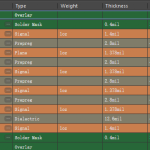
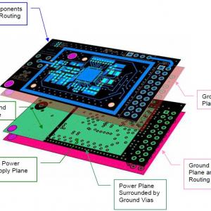
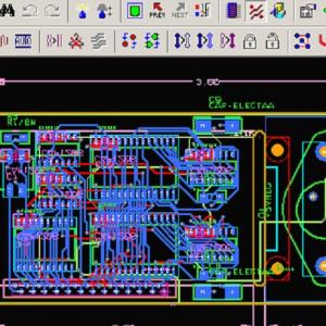
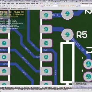
PCB design,How to choose a PCB board,How to avoid high frequency, interference,how to solve the contradiction between manual and automatic routing of high-speed signals,test coupon,high-speed PCB design,the coppering of multiple signal layers be distributed in terms of ground and power supply,Flexible Printed Circuit (FPC) can be designed using the same software used to design PCBs in general. FR-

How to choose the right stacking scheme when designing PCBs

How to choose the right stacking scheme when designing PCBs

2023-02-26

we take four-layer board and six-layer board as an example to introduce their stacking scheme,our GND layer is mainly Our GND layer is mainly placed close to the device layer, this lamination can also do effective isolation for our signal, each lamination scheme has advantages and disadvantages,PCB stacking, higher number of PCB stacking we can also analyse

Illustration: How to identify common SMT polarity components

Illustration: How to identify common SMT polarity components

2023-02-26

Ceramic capacitor without polarity,Polarity components in the entire PCBA,Tantalum capacitor has polarity,PCB negative labeling,SMT table sticker two-terminal diode has polarity,integrated circuit (Integrated Circuit),SOP or QFP type packages are polarised,QFN type packages have polarity,Ball Grid Array

The golden rule of switching mode power supply board layout

The golden rule of switching mode power supply board layout

2023-02-26

It is a step-down switching regulator that supports input voltages of up to 42 V,The most important principle in switching regulator PCB design is that the shorter the alignment for transmitting high switching currents,the input capacitor should be as close as possible to the VIN pin and GND pin of the switching regulator IC,Schematic diagram of a step-up switching regulator, circuit board of the

How are stamped hole packages made in PCB design?

How are stamped hole packages made in PCB design?

2023-02-26

PCB design in the stamp hole package how to make,Stamped hole splicing board, PCB splicing can be used stamp hole technology or double-sided engraved V-slot partitioning technology,a stamp in the division of the round hole design,in the division of the round hole design, the advantages of its strength than V-Cut good

Information sharing RF PCB layout and circuit optimization

Information sharing RF PCB layout and circuit optimization

2023-02-26

PCB layout,circuit,program PCB Layout,program PCB Layout when the double-layer board and 4-layer board layout is predominant,top down are Signal, GND, POWER, GND 4-layer board, placed between the 2 GND a power layer,4-layer PCB is usually 1.6mm thick,single-chip transceiver program PCB Layout

SMT patch process and precautions

SMT patch process and precautions

2023-03-10

the modern electronic assembly industry,Bare Board LoadingSolder paste printing,The first operation of Printed Circuit Board (PCB)" entering the SMT production line is "solder paste (solder paste)", the stencil on the pads/pads of the parts to be soldered on the PCB, fix the electronic parts,Solder paste inspection machine (solder paste inspector, SPI),Fast punching machine,Pick and Place general

104 PCB layout circuit skills Q & A, help you draw the board without worry!

104 PCB layout circuit skills Q & A, help you draw the board without worry!

2023-04-18

PCB board thickness ,in the high-speed multilayer PCB design, how to distinguish between digital and analog ground?multi-layer board layout, because the power supply and ground layer in the inner laye,analog and digital circuits in the PCB board design, high-frequency signal ,Impedance matching of signal lines,the ground plane isolates the analog signal from other digital signals;

< 12345 ... > 11

Product Categories

  • PCBA
  • Rigid PCB
  • HDI PCB
  • Rigid Flex PCB
  • Flex PCB
  • High Frequency PCB
    • Rogers PCB
    • Isola PCB
    • Arlon PCB
    • Nelco PCB
    • Taconic PCB
    • Teflon PCB
    • Neltec PCB
  • Metal Core PCB
    • Aluminium PCB
    • Copper PCB
  • Ceramic PCB
  • Laser Stencil
  • Reverse engineering
  • Purchasing components

Links

Google.comBaidu.com

内页左侧广告1

Feedback

Contact Us

sales@key-pcba.com

234123644@qq.com

Commercial and Cultural Building, Community 11 of Tangwei,Fuhai Street, Bao'An District Shenzhen 518103 GuangDong China.

WECHAT

Copyright © 2016 KEY TECHNOLOGY(HK)CO. ,LIMITED All Rights Reserved.

  • Skype.
  • E-mail
  • Whatsapp
  • Inquiry