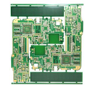
In-depth explanation of PCBs and how to fix PCB warpage?
repairing PCB warpage,PCB production,PCB process PCB warpage repair,warped PCB,baking temperature,wave soldering it,glass transition temperature,PCB circuit board is one of the indispensable components of electronic equipment, many friends are to PCB production, PCB engraving, etc.