
Key Differences Between 1st, 2nd, and 3rd-Order HDI Boards
For professionals in PCB design, procurement, hardware engineering, and process engineering, the concept of HDI "tiers" (or "orders") is often confusing in daily work:What exactly are 1st-tier, 2nd-tier, and 3rd-tier HDI?
Does a higher layer count automatically mean a higher tier?
How can you quickly distinguish between them by looking at blueprints or cross-sections?
Today, we’ll explain this clearly—straight to the point and packed with practical info—so you’ll never be confused again!
Start with the key takeaway (the most important point):
HDI "tier" ≠ Total number of board layers
The sole criterion: The number of laser-drilled blind via build-up/lamination cycles and the number of layers the blind vias span.
✅ 1st-tier = 1 cycle of laser build-up for blind vias
✅ 2nd-tier = 2 cycles of laser build-up for blind vias
✅ 3rd-tier = 3 cycles of laser build-up for blind vias
I. Detailed Definitions & Stack-up Structures for HDI Tiers
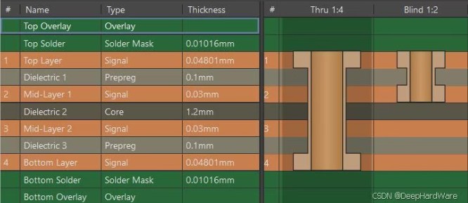
1. 1st-tier HDI (Basic version)Standard stack-up: 1+N+1
Involves only one build-up cycle and one laser drilling process; blind vias connect only the outer layer to the adjacent second layer.
2. Second-order HDI (Advanced Version)
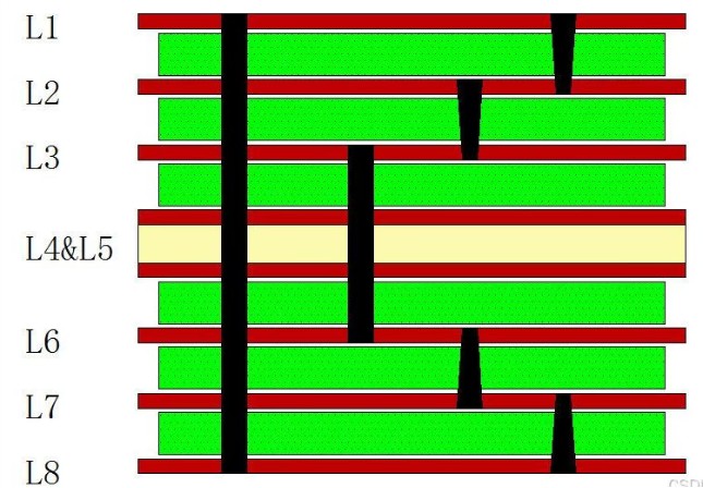
Standard stack-up: 2+N+2
Involves two lamination cycles and two laser drilling stages; blind vias can extend to the third layer.
Supports staggered and stacked via structures, significantly increasing routing density.
Examples of common stack-ups:
6-layer board: 2+2+2
8-layer board: 2+4+2
Features: High density and stable performance; currently the mainstream choice for high-end consumer electronics.
Applications: High-end smartphones, tablets, thin-and-light laptops, and standard precision BGA boards (0.4mm pitch).
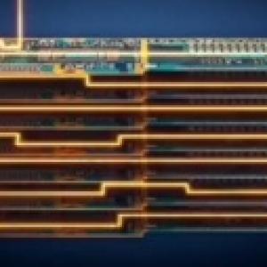
Schematic diagram of second-order HDI structure.
3. 3rd-Order HDI (High-End Version)
Standard Stack-up: 3+N+3
Three lamination cycles and three laser drilling cycles; blind vias can extend down to the fourth layer.
Supports vertically stacked vias and near-arbitrary layer interconnection; maximizes routing capabilities.
Common stack-up examples:
8-layer board: 3+2+3
10-layer board: 3+4+3
Characteristics: High manufacturing complexity, high cost, and extremely high precision.
Applications: 5G equipment, AI computing boards, high-end flagship chip boards (BGA pitch ≤ 0.3mm).
II. 3 Quick Ways to Distinguish (Practical for Field Use)
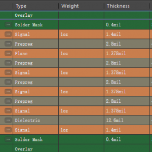
1. Check the stack-up drawing (Fastest)- 1st-Order: 1+N+1
- 2nd-Order: 2+N+2
- 3rd-Order: 3+N+3
- 1st-Order: Only L1-L2 (outermost single-layer) blind vias; no stacking.
- 2nd-Order: Features two levels of blind vias (L1-L2 and L2-L3); can be staggered or stacked.
- 3rd-Order: Three levels of progressive blind vias (L1-L2-L3-L4); clear vertical via stacking.
- Standard industrial control, low-end digital devices → 99% 1st-Order.
- High-end smartphones, portable digital devices → Mostly 2nd-Order.
- 5G, AI, ultra-precision chip boards → 3rd-Order (High-End) HDI.
III. 2 Common Pitfalls for Beginners
Wrong Pitfall 1: More layers mean a higher orderCorrect view: Layer count and order are unrelated!
A 6-layer board can be either 1st-Order (1+4+1) or 2nd-Order (2+2+2); the key factor is the number of blind via lamination cycles.
Wrong Pitfall 2: More vias mean High-Order HDI
The correct understanding: It is based on the number of independent laser build-up cycles, not the total number of holes.
Summary
To put it simply:HDI tier classification is determined by the number of "laser blind via lamination cycles," not the total number of board layers.
Tier 1 (single-layer blind vias), Tier 2 (two-layer staggered/progressive vias), and Tier 3 (multi-layer stacked vias) cater to a full spectrum of needs, ranging from standard to high-precision applications.
Refer directly to this guide when reviewing blueprints, verifying manufacturing processes, or preparing price quotes in your future work—and you’ll never make a mistake again!