How exactly does DRAM work? Within a single chip, how is a single bit
How exactly does DRAM work? Within a single chip, how is a single bit "stored, read, and then restored"? (Part I)
Over the past two years, the surging demand for AI servers, HBM (High Bandwidth Memory), and data centers has transformed DRAM from what was once simply "computer memory" into something far more significant. As the need for high-bandwidth memory grows rapidly, shifts in supply and demand across the DRAM value chain have begun to directly impact the broader semiconductor market. Yet, a closer look at DRAM technology and product architecture reveals a fascinating question: at its most fundamental level, a DRAM cell consists of just "one transistor and one capacitor." How can such a simple structure store tens of gigabytes—or even more—of data? More importantly, the electrical charge stored within a DRAM cell is not permanent; it leaks over time, can be disturbed during read operations, and requires constant "refreshing." Therefore, truly understanding DRAM goes beyond simply knowing what "1T1C" stands for. The real challenge lies in grasping how an infinitesimal, decaying charge can be reliably interpreted as a 0 or a 1, and how these units are organized into a high-speed, functional memory chip.
The Core Structure of DRAM: 1T1C
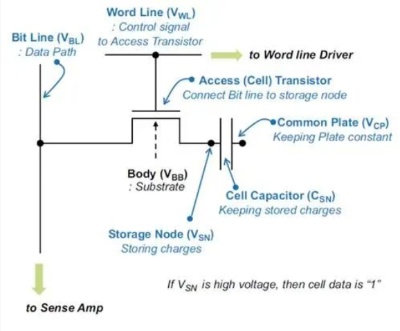
The fundamental storage unit of DRAM (Dynamic Random Access Memory) typically employs a "1T1C" (1 Transistor + 1 Capacitor) architecture, consisting of:
- Cell Capacitor: Responsible for storing electrical charge.
- Access Transistor: Controls when the capacitor connects to the bit line.
- WL (Word Line): Connected to the gate of the access transistor; it controls whether the transistor is turned on or off.
- BL (Bit Line): Used for reading and writing data, serving as a vital signal path between the cell and the peripheral sense amplifier.
- Storage Node: Connected to the cell capacitor; this is the node that actually holds the electrical charge state.
When the WL is pulled to a high voltage, the access transistor (typically an NMOS) turns on, establishing a connection between the storage node and the bit line, thereby enabling read or write operations.
Overall Structure of a DRAM Chip
However, there is a technical detail here that is easily overlooked. If one wishes to charge the storage node to a high level approaching VDD, a standard NMOS transistor presents an issue: the threshold voltage (Vth) drop. Specifically, if the gate voltage is capped at VDD, then as the source voltage rises, the gate-to-source voltage (VGS) decreases; consequently, it becomes difficult to drive the storage node all the way to VDD. For this reason, practical DRAM designs typically employ a "boosted" word line voltage (VPP)—a voltage higher than VDD—to eliminate the Vth drop across the access transistor, allowing the storage node to reach a level much closer to VDD.
This highlights an important fact: the "0s" and "1s" in DRAM are not merely defined by whether a transistor is in an ON or OFF state; rather, they are determined by the amount of charge stored within the cell capacitor. However, a capacitor is not an ideal, permanent "charge reservoir." Even when the access transistor is turned off—effectively isolating the storage node from the bit line—charge cannot be retained indefinitely. In real-world devices, various leakage paths—such as subthreshold leakage and junction leakage—persist. This is precisely why DRAM requires periodic refreshing.
DRAM Read Operation
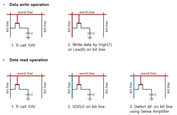
1. Precharge: Bringing the Bit Line to VDD/2
Before a read operation begins, a typical DRAM system precharges the bit line to a reference state—usually VDD/2. Why VDD/2, rather than 0V or VDD? Because regardless of whether the cell stores a "1" or a "0," this midpoint allows the bit line voltage to shift either upward or downward:
- Cell = 1 → The bit line (BL) shifts upward from VDD/2.
- Cell = 0 → The bit line (BL) shifts downward from VDD/2.
In this way, the sense amplifier only needs to detect the direction of the shift, rather than having to distinguish between a full-scale VDD or 0V signal. Standard DRAM read operations follow this established sequence: Precharge → Charge Sharing → Sense → Restore.
2. Word Line (WL) Activation: Connecting the Cell to the Bit Line
The word line is driven high, turning on the access transistor. At this point, charge sharing occurs between the cell capacitor and the bit line. For example, if a cell currently stores a "1": Cell is at a voltage close to VDD, while the bit line (BL) is at VDD/2.Once they are connected, charge redistribution occurs, causing the BL voltage to rise slightly from VDD/2. Conversely, if the cell stores a "0," the BL voltage drops slightly. The resulting voltage difference—denoted as ΔV—is very small, yet it is precisely the signal that the sense amplifier must capture.
3. Sense: The sense amplifier amplifies the tiny ΔV.
This is the most critical step in a DRAM read operation. The sense amplifier detects a minute voltage difference between the bit line (BL) and the reference side, then uses positive feedback to rapidly amplify it to a full logic level—either $V_{DD}/2 + \Delta V \rightarrow V_{DD}$ or $V_{DD}/2 - \Delta V \rightarrow 0V$. Thus, a DRAM read operation is essentially a process of analog signal generation, followed by analog differential sensing, and finally a digital decision; the memory cell does not directly output a complete "0" or "1."
4. Restore: The data must be written back into the cell after a read.
This is a point that often causes confusion when comparing DRAM to many other types of memory. During a read operation, "charge sharing" occurs between the memory cell and the bit line, which disturbs the cell's original charge state. Once the sense amplifier drives the bit line to either $V_{DD}$ or $0V$, the full logic level is written back into the cell because the word line (WL) remains in an active state. Consequently, a DRAM read operation consists of a sequence—Read + Sense + Restore—which is why DRAM is classified as a type of "destructive read" memory.5. PRE (Precharge): Closing the row in preparation for the next access.
Once the current access is complete, the word line (WL) is de-asserted (brought low), isolating the memory cell from the bit line (BL) once again. Subsequently, the precharge circuitry restores the bit line to a voltage level of $V_{DD}/2$, returning the entire array to its initial state.
DRAM Read/Write Operations
DRAM Write Operation
A write operation can be understood even more simply. While a read operation involves the memory cell "influencing" the bit line—with a sense amplifier subsequently determining the state—a write operation entails the peripheral "write driver" actively driving the bit line to a target data state, which is then written into the cell. For instance, to write a "1": the write driver pulls the bit line (BL) high, the word line (WL) is activated, the access transistor turns on, and the cell capacitor charges, ultimately storing a high voltage level. To write a "0": the write driver pulls the bit line low, the word line is activated, the access transistor turns on, and the cell capacitor discharges, ultimately storing a low voltage level.In short, a read operation is the cell "telling" the peripheral circuitry what its state is, whereas a write operation is the peripheral circuitry "telling" the cell what its state should be.
It is evident that the sense amplifier plays a critical role in both read and write operations. Given similar conditions, a larger cell capacitor—relative to the bit line's parasitic capacitance—results in a more pronounced voltage shift on the bit line following charge sharing, making it easier for the sense amplifier to reliably distinguish between a 0 and a 1. This highlights a core challenge in DRAM scaling: as cells shrink, their charge-storage capacity diminishes, yet the bit line remains subject to unavoidable parasitic capacitance, coupling, and noise. This leads to a fundamental question: if a cell can only induce a minuscule voltage difference on the bit line, how can the sense amplifier reliably translate that into a definitive 0 or 1? In the next installment, we will take a detailed look at the true "core amplifier" of DRAM—the sense amplifier.