Understanding the Full DDR Read/Write Process: From a Single Capacitor to Charge and Discharge
A server memory module looks highly sophisticated—featuring a PCB, memory chips, gold contacts, registers, SPD, PMIC, and more—but if you strip it down to its most fundamental level, you find a "tiny capacitor" that is prone to leakage and somewhat temperamental.Its operation can be crudely summarized as follows: the presence of a charge in the capacitor represents one state, while a lack of charge represents another. A transistor acts as a gatekeeper: when the gate is open, charge can flow in or out; when the gate is closed, the capacitor must struggle to hold onto its charge on its own.
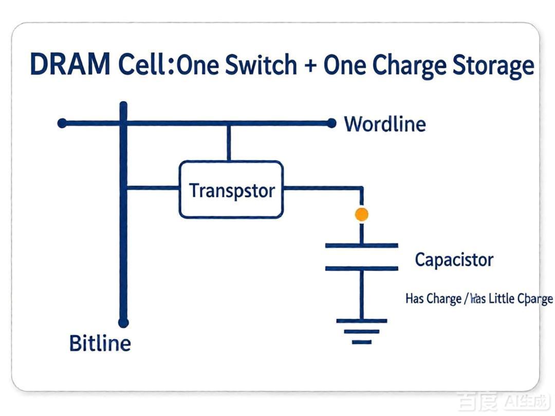
I. 1T1C: A "Minimalist Studio Apartment" for a Single Bit
A DRAM storage cell is known as "1T1C": one switching transistor and one storage capacitor.One terminal of the switching transistor connects to the capacitor, while the other connects to the bitline; the gate is controlled by the wordline. When the wordline is driven high, the transistor turns on, connecting the capacitor to the bitline. When the wordline is turned off, the capacitor is isolated from the outside, maintaining its state via residual charge.
II. Why Can't the Capacitor Just Sit Still?
The capacitor is like a water cup with a tiny hole at the bottom; the storage node gradually loses charge through paths such as junction leakage in the access transistor and dielectric leakage. Higher temperatures accelerate these leakage mechanisms, making data retention increasingly difficult.This is the origin of the term "Dynamic." DRAM doesn't simply "clock out" after data is written; it requires periodic refreshing. Refreshing doesn't involve the CPU copying and rewriting the entire memory, nor does it require a maintenance worker standing next to every capacitor. Instead, it triggers internal activation and restoration row by row, allowing sense amplifiers to reinforce the 0s and 1s in that row.
Here is the first counter-intuitive point: DRAM requires constant activity to retain data. While it appears to be performing "static storage," the chip is actually periodically "rescuing" the charge internally.
III. Why Must the Bitline Be Set to VDD/2 Before Reading?
Now for the truly fascinating part. Before reading a cell, the bitline isn't left floating, nor is it pre-set to 0 or VDD. Instead, precharge and equalization circuits bring the bitline pair—BL and BLB—to a level near VDD/2.Why specifically the midpoint value? Because regardless of whether the cell holds a high or low charge, connecting it produces a tiny, opposing voltage shift relative to that midpoint:
High-charge state: Upon connection, the voltage on BL rises slightly above VDD/2; the sense amplifier detects that BL is slightly higher than BLB. When the cell is in a low-charge state, the voltage on the connected bitline (BL) drops slightly below VDD/2, and the sense amplifier detects that BL is at a lower potential than BLB.
The key word here is "slightly." A single bitline connects to numerous cells, and the metal lines, junctions, and circuit inputs create significant parasitic capacitance, whereas the capacitance of an individual cell is very small. Consequently, connecting the two does not result in a dramatic scenario where the cell instantly pulls the entire bitline from 0.5VDD up to VDD; instead, only a minor voltage shift occurs.
ΔV ≈ (Vcell − Vpre) × Ccell / (Ccell + CBL)
This approximation reveals the inherent trade-offs in DRAM array design: facilitating easier sensing requires large cell capacitance and low bitline capacitance; increasing density demands the smallest possible cells; and connecting more cells to a single bitline saves peripheral circuit area but increases bitline capacitance and reduces sensing margin. Chip engineers must constantly balance these competing factors.
IV. What actually happens internally during a single read operation?
① Precharge: BL/BLB ≈ VDD/2② Row Activation: Wordline opens
③ Charge Sharing: Generation of a tiny ΔV
④ Sense Amplification: Driven to full logic levels
⑤ Column Selection: Data sent to I/O
1. Precharge: Resetting the track to the starting line
When a row is inactive, the precharge circuit equalizes the bitlines (BL and BLB) to approximately VDD/2. You can think of this as placing two competitors at the same starting line before a race begins. As soon as one side pulls slightly ahead, the sense amplifier can determine the direction.2. Row Activation: Opening the entire row, not just reading specific data
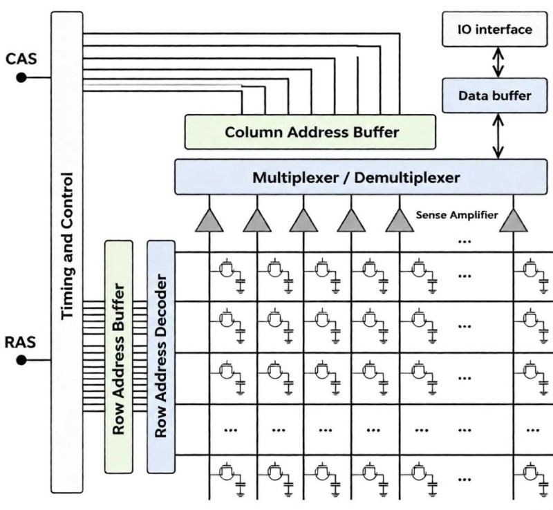
After the memory controller issues an ACT command and provides the row address, the Row Decoder selects a specific wordline. The access transistors for the selected row turn on simultaneously, connecting numerous memory cells to their respective bitlines. A crucial point here is that ACT activates an entire row, rather than just opening the specific bits the CPU ultimately requires.Consequently, DRAM arrays inherently operate on a "row-first, column-second" basis. Once a row is sensed and latched into the sense amplifier array, it forms what is commonly known as the "row buffer." If the same row is accessed subsequently, only the column address needs to change, resulting in much higher efficiency; however, accessing a different row requires closing the current row, performing a precharge, and then activating the new row.
3. Charge Sharing: A "merging" of the capacitor and the bitline
Once the wordline opens, charge sharing occurs between the cell capacitor and the bitline. If the cell's initial voltage is high, the bitline is nudged upward; if the initial voltage is low, the bitline is nudged downward. This change can be minute and is compounded by factors such as device mismatch, noise, coupling, leakage, and process variations.In other words, the sense amplifier does not receive a booming "I am a 1," but rather a faint whisper muffled by three walls. The amplifier must then make a rapid decision without undue hesitation.
4. Sense Amplification: Determining the outcome from mere millivolts
Bitline sense amplifiers typically employ a cross-coupled latch structure. As soon as a tiny differential emerges between BL and BLB, positive feedback drives the "slightly higher" side up and the "slightly lower" side down, ultimately establishing a differential state that approaches the full power supply rails. It performs three tasks in a single operation:First, sensing: determining which charge state the cell is closer to;
Second, amplification: amplifying the minute differential signal to full logic levels;
Third, latching: holding the data for the entire row in the sense amplifier array while that row remains active.
5. Column Selection: Only the required columns are transmitted.
An entire row has already been opened and latched into the Row Buffer, yet the CPU typically requires only a small segment of that data. At this stage, the column address enters the Column Decoder or Column Address Buffer; a multiplexer selects the target column, and the data passes through local I/O, global I/O, data buffers, and output drivers before finally being transmitted via the DQ pins.Thus, a READ command is akin to asking, "Read out a specific line of text from the page that is already open," whereas an ACT command is equivalent to "Opening a specific page." Many beginners learning DDR timing mistakenly view a READ operation as a direct path from the memory cell to the DQ pin, which makes parameters like tRCD, tRAS, and tRP seem daunting. Distinguishing between "opening the row" and "selecting the column" makes the entire protocol much easier to comprehend.
V. Why is DRAM reading considered "destructive"?
When the memory cell connects to a bitline pre-charged to VDD/2 and charge sharing occurs, the cell's original voltage is altered. In other words, the act of reading itself disturbs the storage node. DRAM cannot simply glance at the data from a distance like reading a house number; it is more like connecting a cup to a large water pipe to determine how much water is inside—you get the measurement, but the water level in the cup changes in the process.Consequently, after the Sense Amplifier makes its determination, it drives the bitline to a full high or low voltage level. Since the wordline remains open, this full voltage level feeds back through the access transistor into the cell, performing a "Restore" operation on the storage capacitor: recharging it for a high state or pulling it down for a low state.
A summary to remember: A DRAM read operation is not merely a "glance"; it involves disturbing the data, determining the original value based on minute differences, and immediately writing it back to a stable state.
This is also why tRAS is not a parameter that can be arbitrarily shortened. After an ACT command, sufficient time must be allowed for sensing, amplification, and restoration. If pre-charging occurs too early—closing the wordline and equalizing the bitlines before the cell has fully recovered—the data retention margin will be compromised.