
In-depth Special Report on HDI Substrate Technology
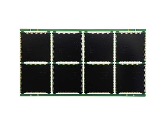
HDI (High-Density Interconnect) is a PCB (Printed Circuit Board) technology characterized by high density; it primarily achieves interconnection between internal copper layers using micro-blind via and buried via technologies. As a critical interconnect component in electronic products, HDI boards are seeing continued market demand growth driven by the trend toward thinner, lighter, and higher-performance electronics. Companies in the HDI sector are actively expanding production capacity and upgrading technology, positioning themselves to benefit from this industry growth.
HDI Overview
A PCB is a printed board featuring point-to-point connections and printed components formed on a common substrate according to a predetermined design; its primary function is to connect various electronic components into a specific circuit, acting as a medium for signal transmission. PCBs are essential interconnect components for assembling electronic parts; they not only provide electrical connections for components but also facilitate functions such as digital and analog signal transmission, power supply, and the transmission and reception of RF/microwave signals. Because they are required in the vast majority of electronic devices and products, PCBs are known as the "Mother of Electronic Products."The manufacturing quality of a PCB directly affects both the reliability of the electronic product and the integrity of signal transmission between chips; consequently, the development level of the PCB industry serves as an indicator of the pace and technological sophistication of a country or region's electronic information industry. The subject of our analysis today is HDI, a PCB technology characterized by high density.
micro-blind vias and buried/blind vias are generally created through a build-up process.
Based on the number of build-up layers, HDI is classified into First-order, Second-order, Third-order, and "Any-layer" HDI (the highest tier of HDI, hereafter referred to as "Any-layer").
Key Characteristics of HDI
The primary characteristic of HDI is high density.Due to the presence of numerous micro-blind vias and buried/blind vias, HDI offers higher routing density compared to through-hole boards. The underlying principle is as follows:
Blind/buried vias save routing space.
Standard multilayer boards use through-holes to connect different layers, but these holes consume significant space that could otherwise be used for routing.
Conversely, using blind/buried vias to establish inter-layer connections frees up space for additional routing, thereby increasing routing density.
Laser drilling enables smaller via diameters.
Blind/buried vias are typically formed by using lasers to ablate the resin dielectric layer, whereas through-holes are usually created via mechanical drilling (as laser drilling struggles to penetrate copper surfaces or is extremely time-consuming).
Therefore, the greater the number of blind/buried vias, the higher the density; in other words, a higher HDI order corresponds to higher density, with "Any-layer" representing the highest-density HDI board type.
However, it is worth noting that once HDI evolves to the "Any-layer" stage, routing density can no longer be increased simply by adding more blind/buried vias; consequently, industrial manufacturing relies on the foundational HDI process... Higher-density boards—specifically Substrate-like PCBs (SLPs)—are manufactured by adopting the modified Semi-Additive Process (mSAP) and substrate-based manufacturing techniques; this demonstrates that HDI technology is a crucial solution for achieving high-density interconnects.
Key Application Areas for HDI
In terms of applications, demand for HDI is steadily rising in the data communication, automotive, and consumer electronics sectors.
HDI PCBs were initially used primarily in high-tech fields such as aerospace and defense; however, as technology has become more widespread and costs have decreased, their use has expanded into consumer electronics, communication equipment, and automotive electronics.
Their primary advantages include smaller dimensions, higher component density, improved signal integrity, and enhanced electrical performance.
These characteristics make HDI PCBs particularly suitable for electronic products requiring compact, lightweight, and thin designs—such as smartphones, tablets, and wearable devices—as well as for high-performance computing and data center equipment.
High-speed communication products (such as those involving AI) are characterized by high on-board signal volumes; historically, high-layer-count boards were the standard choice for these applications.
Taking communication equipment and server/storage devices—which also require high-speed capabilities—as examples: communication equipment predominantly utilizes 8-to-16-layer boards, while server/storage devices primarily use 6-layer and 8-to-16-layer boards.
So, why is HDI technology—originally used in consumer electronics—being introduced into the high-speed communication sector? The key drivers are increased bandwidth requirements and chip technology upgrades.
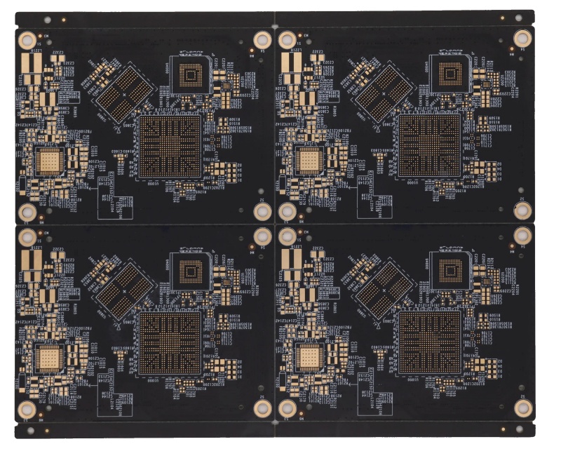
HDI Manufacturing Process and Classification
Manufacturing Process
The manufacturing process for HDI (High-Density Interconnect) boards is complex and intricate, involving several key steps:Raw Material Preparation: Includes materials such as nickel-copper foil, thin multilayer laminates, and prepreg.
Circuit Design and Production: Designing circuit patterns for both outer and inner layers; involves processes such as copper plating, photolithography, stripping, and etching.
Multilayer PCB Fabrication: Assembling the multilayer board according to the design and establishing electrical connections between inner and outer layers.
Surface Treatment and Testing: Performing surface treatment and testing on the completed HDI board to ensure performance and quality.
Laser Via Formation: Utilizing laser drilling technology to achieve high-density interconnection, meeting market demand for thinner, lighter, and more compact electronic products.
Plating and Stacking: The plating stage connects electronic components and provides conductive paths, while the stacking stage involves laminating multiple circuit layers together.
Laser Via Capping/Venting: Creating tiny vents on the circuit board to relieve internal stress and enhance the HDI board's heat resistance and mechanical strength.
Other Key Steps: Includes material cutting, inner-layer dry film application, black/brown oxide treatment, lamination, blind and buried via drilling, electroless copper deposition and copper thickening, and a second inner-layer dry film process.
Classification: HDI boards are classified based on the number of lamination and laser drilling cycles:
First-Order HDI
Connects inner layers to outer layers via blind vias; features lower complexity and interconnection capability, requiring only one outer-layer copper foil lamination cycle.
In summary, the process involves one initial substrate lamination, one drilling cycle, one outer-layer copper foil lamination, and one laser drilling cycle.
Second-Order HDI
In addition to connecting inner layers to outer layers, it incorporates buried via connections, enabling higher routing density and more complex circuit designs. The overall process requires two lamination cycles for the outer copper foil layers (involving two lamination steps, two mechanical drilling steps, and two laser drilling steps).Taking an eight-layer board with blind and buried vias as an example: the core (layers 2–7) is laminated first, and the through-vias and buried vias within these layers are formed; then, layers 1 and 8 are added and laminated, and through-vias spanning layers 1–8 are drilled to complete the board.
The principles behind 3rd-order and 4th-order HDI are similar to those of 2nd-order HDI, but they involve additional outer-layer lamination and laser drilling steps, resulting in higher circuit density.
Any-Layer HDI involves sequential laser drilling and layer-by-layer lamination, representing the highest level of complexity in terms of circuit density and manufacturing difficulty.
SLP technology builds upon Any-Layer HDI by employing the modified semi-additive process (mSAP), allowing for even finer minimum line widths and spacing.
Manufacturing 4th-order and higher HDI boards presents significantly greater challenges.
High-order HDI poses greater challenges regarding interlayer alignment accuracy; during the multiple lamination and laser drilling stages, alignment errors can compromise circuit performance and reliability.
Additionally, the fabrication of blind and buried vias requires high-precision equipment and entails higher costs.
Blind vias, in particular—which connect outer layers to non-adjacent inner layers—add to manufacturing complexity.
The laser drilling process requires precise control to ensure hole quality and consistency, especially when creating deep or micro-vias.
Laser energy control is critical: excessive energy can puncture the copper layer, while insufficient energy may leave residual resin, leading to interconnection failure. Furthermore, the process of filling drilled holes with conductive material (via filling) demands strict quality control, as any defects could impact circuit performance. Challenges of Applying HDI Technology in High-Speed Communication
The manufacturing complexity of HDI for high-speed communication has escalated significantly, potentially reshaping the industry landscape.
Applying HDI technology in the high-speed communication sector presents challenges in three key areas:
Higher HDI layer counts consume more production capacity and demand higher yields at each individual stage.
Based on HDI manufacturing characteristics, blind and buried via structures are created through a sequential build-up process. Each additional layer requires repeating steps such as lamination, drilling, and plating; consequently, upgrading to higher-order HDI involves multiple repetitions of these processes, which reduces overall production capacity.
Achieving a high overall yield for high-order HDI requires extremely high yields at every individual stage. For instance, if the yield for a single stage is 90% (representing the combined yield of processes like lamination, drilling, and plating), the cumulative yield drops to 81% at the second stage and 72.9% at the third stage, and so on. Therefore, high-order HDI places extremely stringent demands on the yields of critical manufacturing processes.
HDI boards used in high-speed communication feature larger surface areas and a higher number of internal layers.
The challenges associated with HDI for high-speed communication extend beyond high layer counts and heavy capacity consumption; they also involve larger board dimensions and a greater number of internal layers. Historically, HDI technology was primarily applied to consumer electronics, where the motherboards inside end-user devices were relatively small. In contrast, samples showcased at NVIDIA’s GTC event reveal surface areas significantly larger than those found in smartphones, imposing stricter requirements regarding board warpage and uniformity. Previously, HDI boards designed for consumer applications prioritized thinness—requiring fewer inner core layers and lightweight, thin materials—meaning that equipment for key processes like drilling, lamination, and plating was optimized for thin boards. However, the high-speed communications sector demands superior dielectric properties, necessitating thicker copper foil, resin, and glass fabric, as well as designs featuring high layer counts (often exceeding ten inner layers). These factors introduce manufacturing challenges distinct from those of consumer products, creating hurdles for the supply chain while simultaneously driving up the value of HDI boards. Leadership by new end-market players is poised to reshape the industry landscape. The structure of the PCB industry is largely dictated by end-market manufacturers; historically, as HDI products were mainly used in consumer electronics, this influence rested with industry giants like Apple and Huawei. Now, however, the key end-market players in high-speed communications are GPU designers such as NVIDIA and AMD. Given the significant process differences between high-speed communication HDI and consumer electronics HDI, these new leaders are likely to introduce new suppliers during the R&D phase. If these new suppliers can keep pace with the client's schedule during mass production, they have a prime opportunity to leapfrog established competitors. Consequently, the traditional HDI landscape may shift; having rapidly advanced their process capabilities and actively seized new opportunities over the past few years, manufacturers from mainland China are already emerging as notable players in the high-speed communication HDI sector. Overall, the introduction of HDI technology into the high-speed communications sector presents new technical challenges while simultaneously boosting the industry's value-added potential and driving growth. At the same time, significant differences in manufacturing processes between HDI for high-speed communications and HDI for consumer electronics—coupled with a shift in the landscape of end-product manufacturers from consumer device designers to AI computing chip designers—mean that changes in the downstream HDI market structure will create opportunities for HDI supply chain players to leapfrog the competition.
Drivers of HDI Growth
AI Servers: High Integration and Complex Interconnect Structures Driving Accelerated Demand for HDIHDI boards represent the fastest-growing segment within the server PCB market.
According to Prismark data, the global market for PCBs used in servers and related system components was approximately $5.177 billion in 2023 and is projected to grow at a rate of 9% to reach $7.974 billion by 2028.
AI servers primarily utilize three types of components—GPU motherboards, OAM accelerator cards, and network interface cards—all of which are expected to transition to HDI technology in the future.
Prismark forecasts a CAGR of 16.3% for HDI from 2023 to 2028, making it the fastest-growing category.
Requirements for PCB specifications have risen significantly due to the demands of AI servers—specifically high-frequency/high-speed signal transmission, high chip integration, complex interconnect structures, and efficient heat dissipation—leading to increased usage of high-end HDI.
While server PCBs were historically dominated by multi-layer through-hole boards, the rapid rise in AI server shipments and increasing technical complexity are changing the landscape.
Taking NVIDIA's AI computing chips as an example, the progression from A100 to H100, and subsequently to B100 and GB200, has seen significant enhancements in chip area, connectivity, bandwidth, and memory capacity.
The GB200 not only delivers 30 times the computing power of the H100 but also vastly outperforms previous generations in memory and bandwidth, necessitating higher PCB specifications.
Demand for High-Frequency, High-Speed Transmission Drives PCB Material Upgrades to M7 and Beyond
The GB200 NVL72 employs advanced NVLink full-interconnect technology; each Blackwell GPU connects to the backplane via high-speed copper cables, achieving bidirectional bandwidth of up to 900 GB/s. High-speed signal transmission necessitates superior material quality and finer manufacturing processes for PCBs to minimize signal crosstalk and ensure signal integrity.
Complex Interconnect Structures
The GB200 NVL72 employs complex backplane connectors and OverPass jumper cables to mitigate high-frequency signal crosstalk on the PCB.
The GB200 NVL72 utilizes NVLink 5.0, achieving a bandwidth of 1800 Gbps and significantly higher transmission rates, making it better suited for HDI (High-Density Interconnect) technology, which supports faster signal transmission.
The use of HDI boards combined with micro-via structures—essential for the complex interconnects of NVLink switch module boards—demands higher precision and reliability during PCB design and manufacturing.
Increased Chip Integration: Boosting System Efficiency and Reducing Energy Consumption
The GB200 chip comprises two B200 GPUs and one Grace CPU; this configuration significantly enhances the chip's computing power and level of integration.
Each B200 GPU contains approximately 208 billion transistors, representing a massive increase in integration density.
To achieve lower power consumption and higher efficiency, the GB200 NVL72 incorporates liquid cooling technology.
This requires the PCB to not only facilitate efficient heat dissipation but also maintain stability and reliability in high-temperature environments.
HDI offers distinct advantages in functional integration and space utilization, leading to increased adoption of high-end HDI boards in the GB200 NVL72.
HDI technology improves routing density, space utilization, and thermal dissipation while offering superior reliability, thereby better meeting the specifications required for AI servers.
Products such as the NVIDIA GB200 NVL72 system are increasing their use of HDI technology.
The GB200 NVL72 consists of 18 Compute Trays and 9 Switch Trays. Each compute tray houses two GB200 superchips and comprises two mainboards, one mid-plane, four network interface card (NIC) boards, and one DPU board; the mainboards, NIC boards, and DPU boards all utilize high-end HDI designs. Each NVLink switch tray contains one NVLink switch module board (utilizing either a high-layer-count or HDI design).
Automotive: Intelligence drives specification upgrades and increased usage volumes.
Compared to standard multilayer boards, HDI boards offer miniaturization and high-density capabilities, along with superior signal transmission performance, making them suitable for applications such as autonomous driving systems, driver-assistance systems, automotive radar, and in-vehicle infotainment systems.
As the automotive industry continues to advance toward electrification and intelligence, the product mix within the automotive electronics PCB sector is evolving, with an increasing share of HDI boards, FPCs (Flexible Printed Circuits), and high-frequency boards.
Intelligent driving systems predominantly utilize HDI boards. LiDAR technology imposes the most stringent requirements—demanding high resolution, strong interference resistance, and compact size—and primarily relies on HDI boards, whereas cameras mainly use rigid boards or rigid-flex boards.
Driven by the increasing sophistication of automotive intelligence, HDI technology is transitioning from 2- or 3-layer-pair (2+N+2 or 3+N+3) structures to 4-layer-pair (4+N+4) or higher configurations to meet the demands of complex sensors and controllers.
Within the automotive PCB market, the share of 4-to-8-layer boards is gradually declining, while the shares of HDI boards and FPCs are rising.
According to TrendForce, in terms of PCB types, 4-to-8-layer boards accounted for approximately 40% of total automotive PCBs in 2023 and are projected to drop to 32% by 2026.
During the same period, the share of HDI boards is expected to rise from 15% to 20%, and the share of FPCs is expected to increase from 17% to 20%. The shares of heavy copper boards and RF boards are set to rise from 8% and 8.8% to 9.5% and 10.8%, respectively, while the share of low-cost single- and double-layer boards is projected to fall from 11.2% to 7.7%. The automotive PCB market is fragmented, with domestic companies making gains across multiple segments. According to Prismark data, the overall automotive PCB market landscape is dispersed. Domestic firms such as Jingwang Electronics and Shihyun Circuits have seen their market shares grow year by year, reaching 6.61% and 3.82% respectively in 2023. In particular, these companies have established a strong presence in automotive HDI technology and maintain long-standing partnerships with major automotive clients, positioning them to benefit from the wave of automotive intelligence.
HDI Competitive Landscape
Manufacturers from Europe, the US, and Taiwan currently dominate the market.According to Prismark data, the top four global HDI manufacturers are Compeq (Taiwan), AT&S (Austria), TTM (USA), and Unimicron (China), with market shares of 10%, 7.7%, 6.7%, and 6.6%, respectively.
Domestic enterprises are accelerating their market presence.
Manufacturers in mainland China involved in the HDI sector—such as WUS Printed Circuit, Shennan Circuits, Shenghong Technology, SYE (Shengyi Electronics), Avary Holding, Founder Technology, Jingwang Electronics, Shiyun Circuits, Chongda Technology, ChaoSheng Electronics, Key Technology and Guanghe Technology—are actively expanding into high-end products.
Domestic manufacturers are aggressively expanding production capacity; customer-related barriers serve as a core competitive advantage.
Certification thresholds for automotive PCBs are high, yet order certainty and profitability are superior. PCBs used in automotive safety components face stringent certification requirements.
Unlike PCBs for consumer electronics, large-scale supply often necessitates dedicated production lines. Certification cycles typically last 2–3 years for overseas Tier 1 suppliers and OEMs, and about 2 years for domestic Tier 1 suppliers and emerging EV makers; PCBs for in-vehicle media—often destined for the aftermarket—typically require 1.5–2 years for certification.
Once a supplier enters the core downstream supply chain, order cycles can extend beyond five years, provided no quality issues arise.
Given these lengthy certification cycles, companies that have already achieved mass production for major automotive clients, secured certification, or possess high-quality customer resources hold a distinct competitive advantage.
In the automotive PCB sector, it is worth focusing on domestic companies that have accumulated years of experience in the automotive field, possess leading technology, and have successfully integrated into the supply chains of major clients. HDI Market Potential
In 2024, global HDI production value is expected to account for approximately 16% of the total PCB market.
From a production value perspective:
Global HDI production value is projected to represent about 16% of the total PCB market in 2024.
The compound annual growth rate (CAGR) for the 2023–2028 period is estimated at 7.1%.
According to Prismark, driven by downstream sectors such as artificial intelligence (AI), automotive, and networking, high-layer-count boards (18+ layers) and HDI boards are set for significant growth in 2024, rising by 21.1% and 10.4%, respectively.
In the medium to long term, high-layer-count boards (18+ layers), IC packaging substrates, and HDI boards will continue to be driven by AI-related industries; their projected CAGRs for 2023–2028 are 10.0%, 8.8%, and 7.1%, respectively—all exceeding the average growth rate.
HDI production value is expected to rise from $10.536 billion in 2023 to $11.628 billion in 2024 (accounting for roughly 16% of the market) and reach $14.826 billion by 2028.
The CAGR for 2023–2028 is estimated at 7.1%.
Downstream demand for high-end HDI capacity is growing at a faster pace.
With the increasing penetration of AI-driven data communications and automotive intelligence, circuit density requirements are rising, necessitating higher-end HDI technology to achieve greater functional integration and performance within limited space.
Consequently, high-end HDI is experiencing faster growth; the market share of HDI products with three or more build-up layers (3+ HDI) is projected to rise from 40% in 2021 to 45% in 2026.
High-end HDI products consume more production capacity, and both capacity utilization rates and profitability are expected to improve further. Based on the HDI manufacturing process, for HDI boards of the same surface area, a higher layer count (or "HDI order") necessitates more repeated processing cycles for the sub-outer layers; consequently, the capacity consumed by processes such as lamination, mechanical drilling, and laser drilling at least doubles. With rising demand for high-order HDI, both HDI capacity utilization rates and output value are expected to increase significantly. Driven by stringent yield requirements and tight production capacity, product profitability is also seeing marked improvement. Upstream materials: CCLs are evolving toward high-speed, high-frequency, and low-loss capabilities. Products driven by AI computing power require upgraded HDI board specifications, which in turn demand that upstream copper-clad laminates (CCLs) deliver high-speed, high-frequency, and low-loss performance. CCLs serve as upstream materials for PCBs, fulfilling three primary functions: electrical conduction, insulation, and structural support. High-speed CCL materials are categorized by dielectric loss levels—ranging from high to low—into Standard Loss, Mid Loss, Low Loss, Very Low Loss, Ultra Low Loss, and Super Ultra Low Loss grades. Upgrades in server platforms are driving the evolution of CCL material specifications. To minimize transmission loss between nodes and ensure signal integrity, it is necessary to reduce transmission loss over distance, a factor determined by dielectric loss. Consequently, the need for higher transmission rates compels the development of higher-speed CCLs; according to data from ITEQ Corporation, PCIe 3.0 utilizes Mid/Low-grade CCLs, PCIe 4.0 requires Low Loss-grade materials, and future PCIe 5.0 applications will adopt Very Low Loss and Ultra Low Loss grades. For instance, NVIDIA’s NVLink 5.0 features higher transmission rates, necessitating higher-grade CCL materials to achieve the required high-frequency, high-speed, and low-loss performance. Regarding the supply landscape for high-speed CCLs, companies from Taiwan and Japan hold the majority market share, while mainland China’s Shengyi Technology is actively expanding its presence to catch up. According to data from Prismark cited in EMC's investor presentation, the high-speed CCL market is currently dominated by EMC (28.4% market share), ITEQ (18%), TUC (16.3%), and Panasonic (10.6%). Domestic manufacturer Shengyi Technology currently holds a market share of approximately 4.4% in the high-speed segment; the company is actively supplying leading domestic and international AI firms, possesses a robust portfolio of high-end products, is making smooth progress in customer adoption, and is poised for continued volume growth.

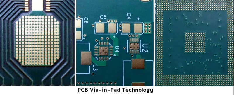
 HDI PCB PROCESS")


