What exactly does ENEPIG protect against? Why isn't ordinary immersion gold plating used on optical module PCBs?
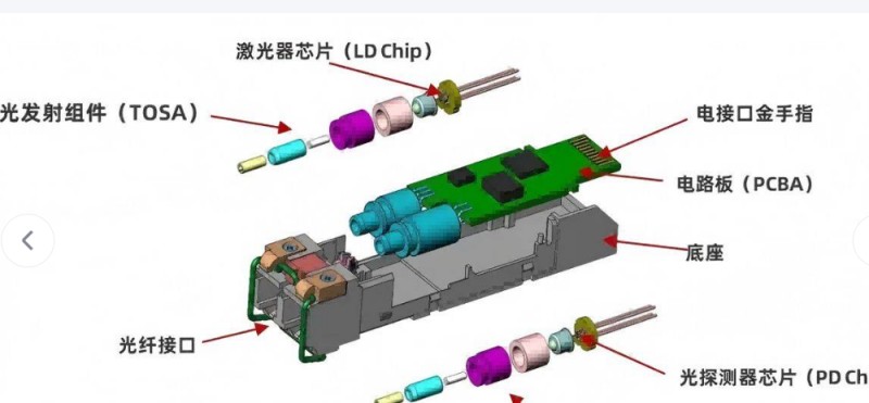
Those familiar with optical modules friends know that the surface treatment process used for the PCB of optical modules is ENEPIG
This is not because it is "superior" to ENEPIG, but because it faces a different connection method.
ENIG's positioning
The standard immersion gold process (ENIG) mainly corresponds to soldering.
During solder paste reflow, the thin gold layer on the surface dissolves into the solder. At this point, the nickel layer and the solder are the ones that actually participate in the interfacial reaction, forming a stable intermetallic compound (IMC).
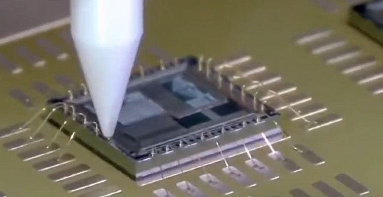
However, on the PCB of the optical module, you will find that in addition to solder paste, some places require gold wire bonding.
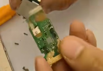
Gold wires are pressed onto the solder pads, and a connection is formed using heat, pressure, and ultrasonic energy.
The gold layer does not melt into the solder as in reflow soldering.
In this case, the gold is left in place, rather than being incorporated into the solder.
Copper / Chemical Nickel / Immersion Gold
This structure works fine during SMT reflow soldering. The gold layer acts as a pre-soldering shield, and during reflow, the gold enters the solder, while the nickel layer absorbs the subsequent interface reaction
Key Issues Preventable with ENEPIG
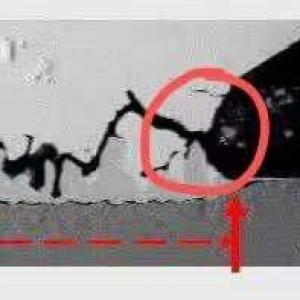
1. Completely Eliminates "Black Pad" Failure: The palladium layer, acting as a dense barrier, prevents the substitution reaction between nickel and gold, avoiding the corrosion of the nickel layer and the formation of "black pads" that occurs in traditional ENIG processes. This fundamentally solves the fatal problems of decreased pad bonding strength and soaring contact resistance.
3. Avoids the Risk of "Gold Brittleness" in Soldering: Only an extremely thin gold layer (approximately 0.1μm) is needed to meet protection requirements. During soldering, excessive gold content at the solder joint will not lead to the formation of a brittle AuSn4 alloy, ensuring the mechanical reliability of the solder joint.
4. Resists Corrosion and Wear in Complex Environments: The three-layer coating provides multiple layers of protection, passing over 1000 hours of salt spray testing. Simultaneously, the coating's wear resistance is significantly improved, making it suitable for repeated plugging and unplugging applications.
Core Reasons Why Ordinary Immersion Gold Plating is Not Suitable for Optical Module PCBs
1. Inability to Meet High Reliability Requirements
If the bonding points between the laser, detector, and PCB of an optical module fail due to a "black disk" defect, it will directly lead to an interruption of optical signal transmission. The "black disk" defect in ordinary immersion gold plating significantly increases the scrap rate in mass production of optical modules, making it completely unsuitable for the stringent reliability standards.
2. Incompatible with micro-pitch, high-frequency designs: The uniformity of ordinary immersion gold plating is weaker than that of ENEPIG plating achieved through full chemical deposition. In scenarios with 0.2mm-level micro-pitch pads and fine lines below 50μm, uneven plating thickness is prone to occur, disrupting the impedance continuity of high-speed signals, causing signal reflection and excessive loss, and failing to support the signal integrity requirements of 100G, 400G, and even 800G optical modules.
3. Insufficient insertion and removal resistance and corrosion resistance: Optical modules need to be repeatedly inserted and removed in scenarios such as data centers and 5G base stations, and are exposed to humid, salt spray, and wide temperature fluctuation environments for extended periods. The wear resistance and corrosion resistance of ordinary immersion gold are far lower than those of ENEPIG, and it cannot guarantee a stable service life of more than 10 years for optical modules.
4. Poor compatibility with multiple processes: Optical module PCBs need to simultaneously perform multiple processes such as chip gold wire bonding, component reflow soldering, and connector soldering. Ordinary immersion gold cannot ensure bonding reliability while preventing "gold brittleness" in thin gold. If selective gold plating is used, the cost will be several times that of ENEPIG, which is completely unsuitable for mass production.