
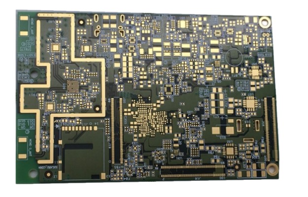
High-speed PCB general layout, circuit principles
High-speed PCB layoutHigh-speed PCB layout basically determines the general direction and structure of the wiring, the division of power and ground planes, and the control of noise and EMI. The general layout principles are -
Understanding the system schematic, dividing the digital, analog, and mixed digital/analog components in each circuit, paying attention to the positioning of the power and signal pins of each chip.
According to the proportion of each part in the circuit, initially divide the wiring area of digital and analog circuits on the PCB, so that digital components, analog components and their corresponding wiring are as far away as possible and limited to their respective wiring areas. After the division is completed, the general order is hybrid devices --> analog devices --> digital devices --> bypass capacitors
Mixed digital and analog components are placed at the junction of the digital and analog signal areas, with the digital and analog pins of the chip facing their respective wiring areas. Pure digital or analog components placed within their respective specified ranges, with crystal circuits as close as possible to their driver components.
Noise-sensitive devices should be kept away from high-frequency signal wiring, such as feedback voltage Fb. Signal wiring with timing requirement restrictions requires adjustment of layout according to length and structure. Bypass capacitors are placed as close as possible to the power supply pins, especially for high frequency capacitors. Place high-capacity capacitors in the power supply interface accessories to keep the power supply stable and reduce low-frequency noise interference.
High-speed PCB circuit
High-speed PCB circuit involves more details and more flexible, with a reasonable layout as the premise, with the basic principles of wiring, allows us to avoid unexpected signal integrity problems or timing problems -
Reasonable choice of layers. High-frequency circuits are more integrated, wiring density is high, the reasonable use of multilayer boards can use the middle layer to set shielding, better grounding, effectively reduce parasitic inductance, shorten the signal transmission length, reduce cross-talk between signals, etc.
Reduce the bending of leads between the pins of high-speed circuit components. High-frequency lines should preferably be fully straight, and when bending is required, 45° fold lines or circular arcs can be used to avoid refraction of signals.
Reducing the length of high-frequency leads.
Reduce the interlayer overlap of high-frequency leads. That is, reduce the overholes used in the alignment process, an overholes can bring about 0.5pf of distributed capacitance, reducing the number of overholes can reduce the impact on the signal speed.
Pay attention to the cross-talk that may be introduced when wiring signal lines in close proximity, and if parallel distribution cannot be avoided, a large area of ground can be arranged on the opposite side of the parallel lines and between the lines. In practice, parallel wiring within layers is almost unavoidable, but the wiring direction of two adjacent layers must be mutually perpendicular, i.e., parallel horizontal and vertical wiring in the direction of the alignment of two adjacent layers, respectively.
Ground-wrapping measures for particularly sensitive signal lines or local units. Such as ground wrapping for clock units.
Signal wiring of all types cannot form loops or current loops.
Proper selection of single-point grounding and multi-point grounding. Low-frequency circuit, the signal operating frequency is usually less than 1MHz, when the wiring and inductance between the devices have less impact, while the grounding circuit to form a loop current on the impact of interference, so the use of single-point grounding; high-frequency circuit, such as when the signal is greater than 10MHz, the ground impedance will become very large, at this time, multi-point grounding should be used to reduce the grounding impedance. About the design of the ground, also need to pay attention to as thick as possible ground, the ground is too thin will lead to grounding potential with the change of current, if possible, the ground home village to be able to pass 3 times the allowable current of the PCB, in addition, the grounding system to form a closed loop can also reduce the potential difference.


