How exactly does DRAM work (Part 2)?
How does a sense amplifier convert a "small signal" into 0s and 1s?
One of the most fascinating components of DRAM is the sense amplifier. Signals emerging from a memory cell are typically extremely small—far from reaching a standard logic level. A simplified view of a DRAM read operation is as follows: Cell → Charge Sharing → tiny ΔV → Sense Amplifier → full 0/1 logic level. The role of the sense amplifier is to rapidly amplify this minute voltage difference. In a typical DRAM architecture, the sense amplifier does not operate on a single bit line in isolation; instead, it employs a pair of complementary bit lines to perform a differential assessment.
Prior to a read operation, the bit lines are precharged to an intermediate voltage level. Once a cell is connected, charge sharing causes a slight voltage shift on one of the bit lines, while the other serves as a reference. The sense amplifier is then tasked with resolving a fundamental question: which side is at a higher potential? If one side is even marginally higher than the other, the sense amplifier leverages a cross-coupled structure to create positive feedback. This amplifies the initial, tiny voltage difference—from a small ΔV to a larger ΔV, eventually reaching VDD or 0—resulting in a full logic level. This is the core function of the sense amplifier: rather than merely "reading" the cell, it performs a "regeneration" based on an infinitesimal signal. Consequently, a DRAM read operation is not a direct output of a 0 or 1 from the cell; rather, it involves the cell creating a minor disturbance, which the sense amplifier then interprets, regenerates via positive feedback, and restores to a full logic level.
A critical aspect of this process is that a DRAM read operation inherently destroys the original state of the cell. This occurs because the cell capacitor must undergo charge sharing with the bit line during the read, which redistributes the stored charge and alters the cell's original state. Therefore, a DRAM read is not a "non-destructive" observation; it is more accurately described as a sequence of: read → evaluate → amplify → restore. Once the sense amplifier has completed its evaluation, it continues to drive the corresponding bit line toward a full 0 or VDD. Micron’s technical documentation on DRAM explicitly characterizes this process as "Read & Refresh"—once the word line is activated, the sense amplifier reads the cell's state while simultaneously restoring the charge back into the cell. Therefore, a sense amplifier effectively performs two tasks simultaneously:
First: Sensing—determining the original data stored in a cell.
Second: Restoring—writing the data back into the cell.
This is why DRAM is often characterized as having a "destructive read" mechanism. The refresh process is also directly related to this mechanism. Because the cells themselves are subject to leakage, the stored data gradually degrades over time. Consequently, DRAM requires periodic access to these cells to restore their contents. From a system-level perspective, a refresh operation is essentially the continuous process of "reading out" degraded data and "restoring" it. Thus, the data retention capability of DRAM ultimately depends not only on the capacitor itself, but also on:
- The amount of charge a cell can store;
- The rate of charge leakage;
- The reliability with which the sense amplifier can detect minute signals;
- Whether the refresh interval meets the data retention requirements.
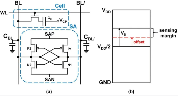
Sense Amplifier Schematic
From Cell to DRAM
If you look at just a single cell, DRAM might seem quite simple. However, a single DRAM chip can contain billions of such cells, which raises a fundamental challenge: how do you precisely locate the specific bit you need among so many cells? Rather than providing a dedicated set of read circuitry for every individual cell, DRAM organizes its cells into a structured two-dimensional array—consisting of "word lines" (rows) and "bit lines" (columns). When a row is selected, all the cells along that row are simultaneously connected to their respective bit lines. Consequently, a DRAM access is not merely a matter of "opening a single cell." The actual process is as follows: a row address is sent to a row decoder, which activates a specific word line; this causes an entire row of cells to be loaded into sense amplifiers. Subsequently, column-related circuitry selects the specific data required from this activated row. This gives rise to a crucial concept in DRAM architecture: the "row buffer." Once a row has been "activated," its data is latched and restored by the sense amplifiers—effectively acting as an "open page" within the current bank. If a subsequent access targets the same row, the entire row-activation process can be skipped; this is known as a "row hit." Conversely, if the access targets a different row, a "precharge" operation must occur (closing the current row and returning the bit lines to a voltage level of VDD/2), followed by the activation of the new row. This is why DRAM performance specifications include parameters like tRCD, tRAS, tRP, and CL—these are not arbitrary figures, but rather representations of the specific physical operations occurring within the DRAM chip. In the DRAM specifications published by manufacturers like Samsung, one can observe the organization in terms of banks, row addresses, column addresses, and page size—where "page size" refers to the amount of data transferred into the internal sense amplifiers following a row activation.
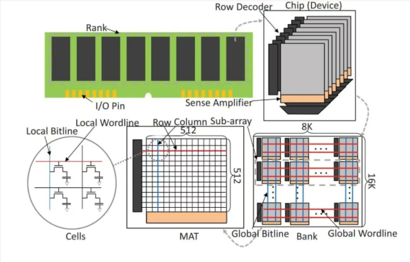
DRAM Array、Sense Amplifier
From the perspectives of manufacturing and circuit design, this architecture presents a practical trade-off: a longer bit line allows for more connected cells—thereby increasing array density—but it also results in higher parasitic capacitance, making it more difficult to detect the minute voltage differential ΔV during a read operation. As noted in documentation from *Semiconductor Engineering*, excessively long word lines and bit lines increase capacitive loading and degrade operating speed. Consequently, practical memory designs are typically partitioned into multiple sub-arrays, each supported by its own row drivers and sense amplifiers. Therefore, increasing DRAM capacity is not as simple as merely "shrinking the cells." A delicate balance must be maintained among cell area, capacitors, access transistors, bit line RC (resistance-capacitance) characteristics, sense margins, and the overall array architecture. This is precisely why the advanced process technologies used for DRAM cannot be simply equated to those used for standard logic devices.
Why is DRAM becoming increasingly difficult to manufacture?
The core challenge in DRAM can be summarized in a single sentence: as memory cells shrink, they must still retain sufficient charge, while the sense amplifier must remain capable of reliably distinguishing these minute signals. Consider the capacitor: its fundamental relationship is defined by the equation C = εA/t. If the lateral area of a cell—and consequently the area of its capacitor—is reduced, the capacitance will inevitably drop. However, DRAM cannot tolerate an indefinite decline in capacitance; since the charge stored in a cell is given by Q = C·V, a reduction in C (assuming other variables remain constant) leads to a decrease in the stored charge. Less charge results in a smaller voltage delta ΔV on the bit line, a narrower sense margin, and, ultimately, a higher risk of read errors. To address this, modern DRAM employs a "three-dimensional" design strategy: shrinking the footprint while increasing the height. This has led to the development of the high-aspect-ratio, cylinder- or container-shaped storage capacitors we see today. As lateral dimensions shrink, the capacitor must extend vertically to maintain the necessary capacitance, resulting in increasingly tall structures.
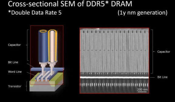
High-aspect-ratio capacitors for modern DRAM
This brings us directly to the challenges of manufacturing: what appears to be a simple "capacitor" is, in reality, a three-dimensional structure with a high aspect ratio. Consequently, continued DRAM scaling requires not only shrinking transistors but also precisely controlling a complex set of parameters for the capacitor—including its aspect ratio, dielectric thickness, leakage, mechanical stability, process window, and parasitic effects relative to adjacent structures.
Meanwhile, as access transistors continue to shrink, potential leakage paths increase, causing the cell’s charge to dissipate more rapidly. This shortens the retention time and necessitates more frequent refresh cycles. This is the true meaning of the "Dynamic" in DRAM: rather than locking data into a permanent, stable state, the system relies on periodic refreshes to restore data as charge inevitably leaks away. Thus, the complete operational logic of DRAM can be summarized as follows:
Write: Storing charge into a cell.
Read: Facilitating charge sharing between the cell and the bit line.
Sense: Using a sense amplifier to detect a minute change in voltage (ΔV).
Restore: Writing the determined logical state back into the cell.
Refresh: Restoring the data before charge leakage causes it to degrade.
Viewed through this lens, the competition in today’s DRAM industry is not merely about who can build the smallest transistor. The real challenge lies in maintaining sufficient charge within an ever-shrinking cell area; preserving an adequate "sense margin" despite increasingly weak signals; and managing manufacturing defects, leakage, and reliability within the tight tolerances required for mass production. Ultimately, what a DRAM chip "stores" is not an abstract 0 or 1, but rather a specific state of minute electrical charge—a state that must be precisely established, detected, amplified, restored, and periodically maintained.