PCB Layout Design for High-Precision ADCs: Key Insights from TI Precision Analog Seminars
Higher resolution exposes PCB layout errors more starkly: 12-bit designs require "caution," 16-bit designs demand "absolute precision," and in 24-bit designs, even the slightest layout oversight will manifest in the data. This article covers LSB size, six fundamental design principles, ground plane management, the thermocouple effect, and nine real-world examples of poor PCB layout—serving as a practical self-check list for high-resolution analog front-end design. (This content draws from the "Precision Analog Applications Seminar" materials by TI.)I. Why "LSB Size" Is Crucial to PCB Layout
Many engineers approach PCB layout by simply memorizing a set of rules—yet, there are almost always exceptions. Rather than merely providing a list of rules, this TI resource establishes a foundational benchmark: exactly how many volts does 1 LSB represent in your system? Depending on the signal range and bit resolution, the LSB size can vary by several orders of magnitude. Whether parasitic layout effects—such as microvolt-level voltage drops or thermoelectric potentials—become critical failures depends entirely on this benchmark.
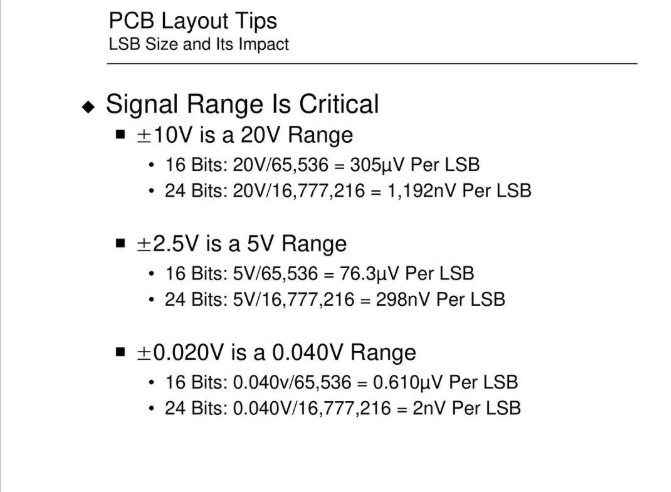
Figure 1 | Page 3 of the original text: LSB size and its implications. For a given full-scale range, the LSB of a 16-bit system differs from that of a 24-bit system by a factor of 256—a key factor in determining whether layout parasitics will be critical.
Let’s first look at three sets of typical calculations:

The impact of these figures becomes clear when viewed through a comparative lens: in a 16-bit system, a ±10 V range yields an LSB of 305 µV, whereas a 5 V range yields only 76.3 µV. Once a programmable gain amplifier (PGA) is introduced—amplifying the signal and utilizing the full input range—the effective resolution can easily degrade until it is swallowed by the system noise. As the input range shrinks and the bit resolution increases, even a microvolt-level loss—which might otherwise be considered "negligible"—can become catastrophic for the design.
Consider a concrete example: a 1-inch-long PCB trace (with a width of approximately 7 mils) using 1/2 oz copper foil will experience a voltage drop of about 1.3 µV when carrying a 10 µA current.
For a 24-bit system with a ±2.5 V range (where 1 LSB = 298 nV), this 1.3 µV drop equates to approximately 4 LSBs.
In a 16-bit system, such a trace warrants serious attention.
Even in a 12-bit system, it is a factor that must be kept firmly in mind.
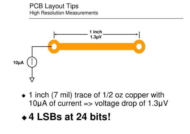
Figure 2 | A 1-inch trace with a 7 mil width and 1/2 oz copper foil carries a 10 µA current, resulting in a 1.3 µV voltage drop—equivalent to 4 LSBs in a 24-bit system.
This establishes a clear hierarchy of difficulty: 12-bit designs require careful layout; 16-bit designs demand that every step be executed correctly to achieve specified performance; and in 24-bit designs, any layout error will manifest directly in the output data stream.
II. Six Fundamental Design Principles
The principles for high-resolution PCB design provided by TI can be summarized into six points, each rooted in a clear physical rationale.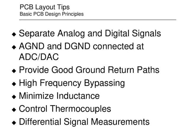
Figure 3 | Six fundamental design principles for high-resolution PCBs. Partitioning, grounding, return paths, bypassing, inductance, and thermal coupling—the order itself reflects their priority.
1. Separation of Analog and Digital Signal Sections
Separate the analog and digital sections on the PCB to keep "noisy" digital switching noise away from low-level analog signals. However, both sections must eventually converge at the ADC/DAC—this is the most critical point in this entire discussion.2. Single-Point Connection of AGND and DGND at the ADC/DAC
Analog ground (AGND) and digital ground (DGND) must be connected at the ADC or DAC chip. The reason: the internal analog and digital components of the device need to communicate, and ground currents require the shortest possible return path. If AGND and DGND are connected elsewhere, these currents are forced to take a longer path, potentially contaminating other circuits along the way.3. Providing a Robust Ground Return Path
The path taken by ground current is determined by impedance. The return path must be kept close to the signal trace; otherwise, the loop area increases, which in turn amplifies all parasitic effects.4. High-Frequency Bypassing (Decoupling)
High-frequency currents require a nearby bypass path. The effectiveness of decoupling capacitors is directly determined by their placement and how they are connected to the ground.5. Minimizing Inductance
Inductance is determined by the size of the current loop. By routing the return current directly beneath the signal trace, the loop area—and consequently the inductance—is minimized. This is the primary value of a solid, continuous ground plane. If a sufficiently continuous ground plane cannot be achieved on a two-layer board, the number of layers should be increased.6. Controlling the Thermocouple Effect
A temperature difference at the junction of any two dissimilar metals generates a thermal electromotive force (the Seebeck effect). This factor is frequently overlooked and will be discussed in further detail later.
III. Recommended Layout Workflow: Partition First, Then Remove Partitions
Regarding the classic debate over "how exactly should analog and digital grounds be connected?", Texas Instruments (TI) offers a highly practical workflow:
1. Begin the layout with partitioned ground planes: route digital signals only over the digital ground plane, and analog signals only over the analog ground plane.
2. As a final step, remove the partitions to create a single, continuous ground plane.
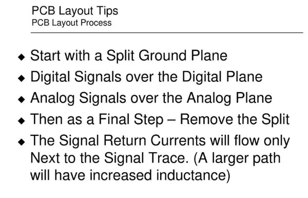
Figure 4 | Recommended layout workflow. Use a split ground plane to constrain the routing paths, then remove the split as a final step—at this point, the signal return current will automatically flow directly beneath the traces.
Why is it safe to use a single, continuous ground plane? Because AGND and DGND are already connected at the ADC/DAC and at the power supply; splitting the plane would actually create ground loops. With a solid, continuous ground plane, analog signal currents flow only within the analog region of the plane, while digital signal currents flow only within the digital region—the two remain effectively separate.
Why don’t these currents stray into the wrong areas? The answer lies in a fundamental physical principle: a larger current path implies higher inductance. Signal currents will always follow the path of least impedance—specifically, the narrowest return path located directly beneath their respective signal traces. A solid ground plane automatically provides this optimal return path for every signal trace, thereby eliminating ground loops.
This explains why using a "solid copper pour" is not merely a formal convention; it is a way to let the laws of physics—rather than the guesswork of a layout engineer—determine the return path.
IV. Layout-Induced Offset Voltage: The Thermocouple Effect
This is one of the most insidious types of layout errors in precision measurement:Whenever two different metals meet, a temperature difference across the junction creates a thermocouple.
PCB vias are no exception—they represent junctions where copper plating meets other metals or solder.
Consequently, if the positive and negative paths of a differential signal have an unequal number of vias, an offset voltage that drifts with temperature will be generated. Factors such as a human hand approaching the board, heat generated by chips, or airflow ensure that temperature gradients are always present, causing this offset to constantly fluctuate.
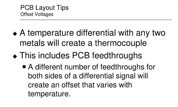
Figure 5 | Thermocouple effect. A difference in the number of vias on either side of a differential signal path introduces an offset voltage that drifts with temperature.
The solution is simple yet easily overlooked: route the two traces of a differential pair side-by-side and in close proximity. This ensures they experience the same thermal gradients and utilize the same number of vias, allowing any thermal electromotive forces (EMFs) to cancel each other out at the differential terminals.
V. Layout Review: Nine Real-World "Bad Examples"
The latter part of the TI material presents a collection of real-world PCB layout critiques—referred to in the original text as a "Rogue's Gallery"—highlighting pitfalls that others have encountered. The illustrations for the following cases are screenshots from the original presentation slides, with the accompanying text representing TI’s original annotations.Case 1: Ground Current Injected into the Crystal Oscillator’s Ground
On one board, the ground current from component U3 was routed into the ground connection point of the crystal oscillator (Y1) capacitor, before eventually merging into the system ground. The result: the crystal oscillator experienced significant interference, leading to a highly unstable clock signal. The lesson: the ground return path for high-current or switching-noise sources must never be allowed to "piggyback" on the ground connection point of a sensitive circuit node.
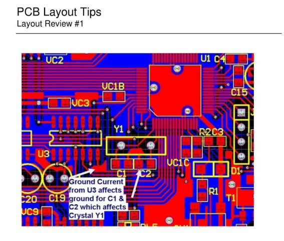
Figure 6 | In Case 1, the ground current from U3 is routed to the capacitor ground connection point for crystal oscillator Y1, and subsequently flows into the system ground, causing clock instability.
Case 2: Sacrificing Performance for the Sake of "Symmetry"
Arranging capacitors and components—or routing traces—to achieve a certain aesthetic symmetry can inadvertently introduce avoidable inductance and resistance, thereby directly degrading system performance. The primary objective of layout is electrical performance, not geometric symmetry.
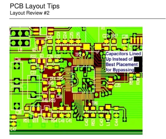
Figure 7 | Case 2: Arranging components with the goal of achieving a symmetrical aesthetic inadvertently introduces excess inductance and resistance.
Case 3: Replacing "routing traces to a single common ground point" with "grounding via nearby vias"
This board features a reasonably complete ground plane; however, instead of connecting components directly to the ground plane via vias, the design routes them—using relatively wide traces—to a centralized grounding point. Conclusion: Even with wide traces, the added inductance and resistance cannot compare to the performance of placing one or more vias directly next to a component’s ground pin to connect it to the ground plane. Adding a few extra vias nearby is always the most cost-effective way to improve performance.
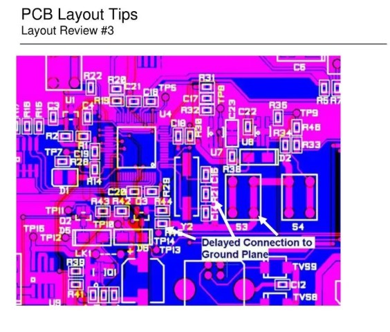
Figure 8 | Case 3: Even when wide traces converge at a centralized grounding point, their inductance and resistance remain higher than those achieved by placing multiple vias in close proximity to the device’s ground pins.
Case 4: "Copper Fill" on the Top Layer Is Not Grounded
The copper pour on the top layer may appear to be merely an "area fill" used to occupy the gaps between traces. If this top-layer copper is not connected to the ground plane on the bottom layer, the ground plane loses a continuous current return path. Conversely, if the copper on the top and bottom layers is connected, the ground return current gains a low-inductance path. Copper pours must be grounded; otherwise, they serve no purpose beyond aesthetics.
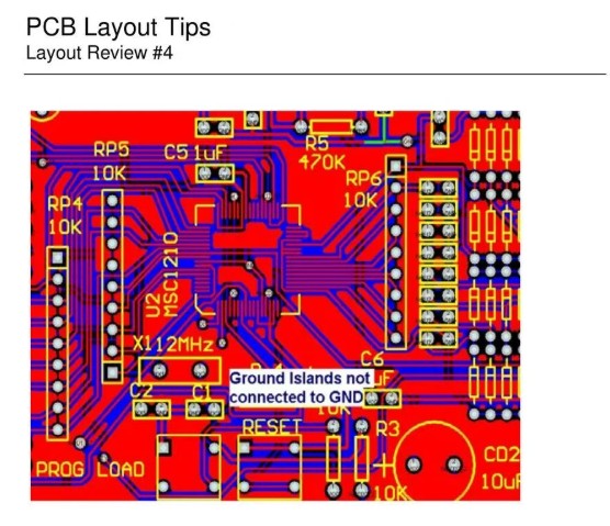
Figure 9 | Case 4: The top-layer copper pour only fills the gaps between traces and is not connected to the bottom-layer ground plane, resulting in the loss of a continuous path for the ground return current.
Case 5: Severe fragmentation of the ground plane. The bottom ground plane exhibits significant segmentation.
A closer look reveals an even more ironic fact: the traces cutting through the ground plane are, in themselves, ground signals. Using traces instead of a solid plane to connect ground points is a classic case of self-sabotage.
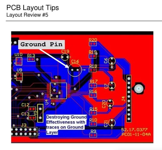
Figure 10 | Case 5: The underlying ground plane is severely fragmented, yet the trace that cuts through it is itself a ground signal—essentially "routing a ground signal across the ground plane."
Case 6: Applying Digital Routing Practices to Analog Boards (Top and Bottom Layer Comparison)
A comparison of the top and bottom layers reveals that some traces could easily have remained on the same signal layer, allowing the ground plane to stay intact. This is a classic issue that arises when digital routing habits are applied to analog boards: while enforcing a uniform routing direction across layers may simplify the layout process, it results in inefficient ground return paths and unnecessary increases in inductance. It bears repeating: inductance is determined by the size of the current loop.
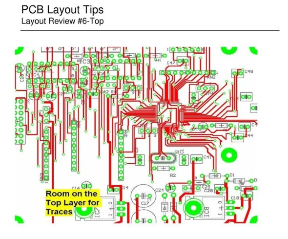
Figure 11 | Case 6, Top Layer: Some traces could have been routed on this layer, which would have allowed for a more intact ground plane.
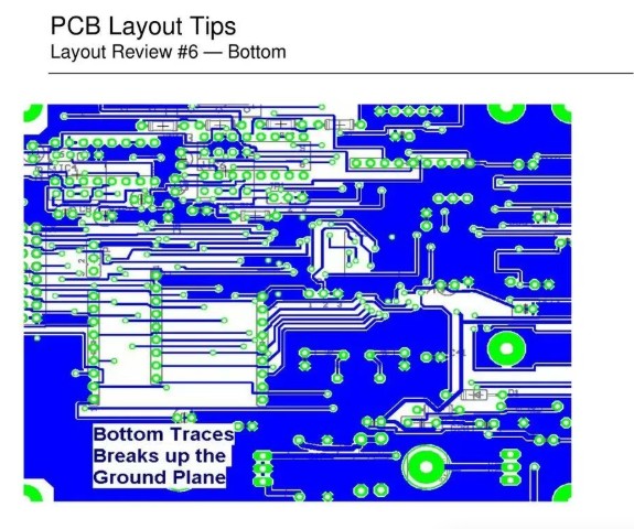
Figure 12 | Case 6, Bottom Layer: Unidirectional routing simplifies the layout but compromises ground return efficiency—inductance is determined by the size of the current loop.
Case 7: Good analog/digital partitioning, but failure to connect grounds at the ADC
While the analog and digital sections of this board are well-separated, the AGND and DGND planes are not connected at the ADC. Proper partitioning is merely the baseline requirement; an incorrect grounding point can still allow noise to couple into the system.
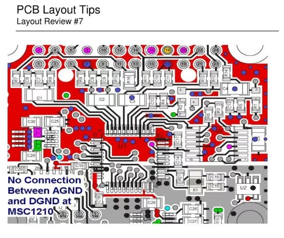
Figure 13 | Case 7: Proper partitioning, but AGND and DGND are not connected at the ADC (MSC1210), allowing noise to couple into the circuit.
Case 8: "Narrow-Neck" Channels in the Ground Plane
While the analog and digital sections are well-separated—with AGND and DGND correctly connected at the MSC1210 via a wide trace—the ground plane contains narrow current channels, which increase both inductance and noise. Specifically, the return current for digital signals—which should ideally flow directly beneath the horizontal signal traces—is forced to take a circuitous path because the available channel in the ground plane runs longitudinally.
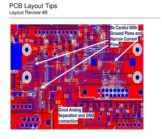
Figure 14 | Case 8: A narrow longitudinal channel in the ground plane creates a mismatch with the requirements for the return current path; the return current is forced to take a detour, leading to increased inductance and noise.
Case 9: Comparison Before and After Rectification (The most instructive example)
Before rectification: Analog and digital sections are separated, with ground planes present on both the top and bottom layers; however, the bottom-layer ground plane is severely fragmented, preventing the ground return current from flowing directly beneath the signal traces.
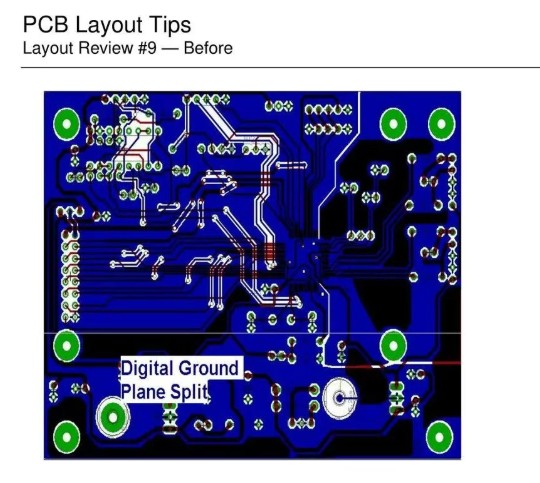
Figure 15 | Case 9, Before Rectification: The ground plane is severely fragmented, preventing the return current from flowing in close proximity to the source signal trace.
After rectification: A few simple adjustments to the routing resulted in a significantly better ground return path.
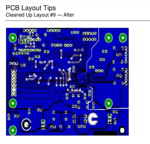
Figure 16 | Case 9 (After Rectification): A few simple adjustments yield a large, continuous ground plane—a larger, more continuous plane means shorter return paths, which in turn results in lower inductance.
In short: a larger, more continuous ground plane means a shorter return path, which results in lower inductance. Often, you don’t need to redesign the entire board; simply moving a few traces that are fragmenting the ground plane to another layer can solve the problem.
VI. The Overlooked Via: A Useless Protective Resistor
Here is a brief, standalone case—distinct from the nine main examples—that warrants its own discussion:The design intent was to use a resistor to protect a chip’s reset pin, and the resistor was indeed placed nearby. The issue, however, is that a via exists along the path leading to an external connector, effectively bypassing the resistor’s protection—leaving the reset pin exposed.
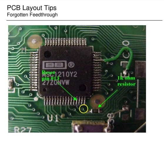
Figure 17 | The Overlooked Via: The placement of the protection resistor is correct, but the via leading to the external connector bypasses it, rendering the protection ineffective.
Lesson: "Placing components nearby" for protection does not automatically guarantee effective series protection. You must verify, point by point along the signal path, that the only available path between the pin being protected and the external environment is indeed through the protection component.
VII. Conclusion: An Actionable Self-Check Checklist
Condensing TI’s findings into a checklist that can be used directly during layout reviews:
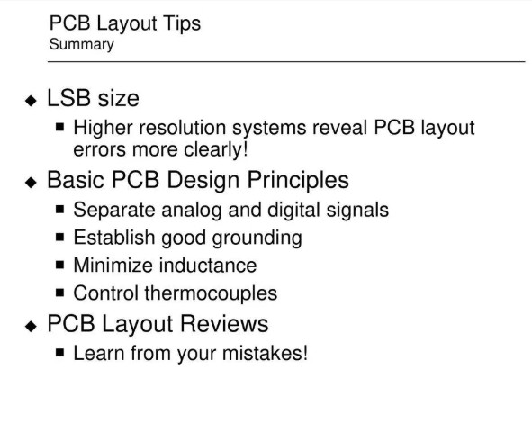
Figure 18 | Summary—The higher the resolution, the more clearly the system will reveal PCB layout errors.
Understanding Resolution
First, calculate the LSB (Least Significant Bit) value: Full-Scale Range ÷ 2^N. Use the benchmark of "1.3 µV/inch (at 10 µA with 1/2 oz copper)" to determine which voltage drops are tolerable.
Higher resolution makes layout errors more apparent—in 24-bit designs, there is no such thing as "close enough."
Grounding and Return Paths
Separate analog and digital routing regions; connect AGND and DGND at a single point—specifically at the ADC/DAC.
Begin the layout process using split planes, then remove the splits in the final step, relying on the principle that current follows the path of least impedance.
Connect device ground pins to the ground plane via vias placed as close as possible; do not use traces in place of planes, and avoid relying on a single, centralized grounding point.
Ensure the ground plane remains continuous—avoid narrow channels or cuts (even if those cuts are intended for other ground connections).
All copper pours must be connected to the ground plane; otherwise, they are effectively non-existent.
Parasitics and Thermal Effects
Inductance is a function of loop area; the return current will always flow directly beneath the signal trace.
Route differential signals side-by-side, ensuring they experience the same thermal gradients and utilize an identical number of vias to cancel out offsets caused by thermoelectric potentials.
Verify that protection or series components are positioned directly along the signal path, ensuring they cannot be bypassed by vias or alternative routing paths.