
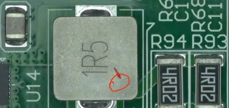
Discussion on the situation of cracks on the surface of power inductors after reflow soldering
Coffee Cake: Dear teachers, this is a power inductor. Have you ever encountered such surface cracks?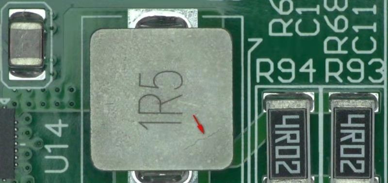
Liu Haiguang: Usually there are defects in the core sintering, the density there is uneven, and stress cracks occur after cooling @coffeecake
Coffee Cake: This is produced after reflow soldering, which is very possible according to what you said. In addition, what other factors do you think may cause this problem?
Liu Haiguang: Is the initial temperature rise rate of reflow soldering normal? That is to say, sudden heat needs to be avoided
Coffee Cake: The soldering curve is normal. Clean after welding and dry at 50 degrees
george tsao: There seems to be signs of swelling. Are the parts wet? , the parts were purchased last year in 2019, right? What month?
Coffee cake: Purchased this year, April and October
Golden Years: There may be problems with the device itself. If there are any micro-cracks before welding, you can use a magnifying glass to check carefully. Generally, they cannot be seen with the naked eye. The cracks will increase after reflow and thermal expansion. Welding generally does not cause damage.
Coffee Cake: I checked the unwelded parts in stock and saw no cracks. Look back and take a closer look at @Jinhuanian
Golden Years: Go through the reflow furnace for a few times without soldering to see if there are any cracks. Are they all from the same batch?
Coffee Cake: Good idea, will try it later, two batches@Jinhuanian
Golden Years: Run a few of the two batches through the reflow oven to see what the results will be for that batch.
Coffee Cake: There is only one batch left, and two batches have been welded together.
Liu Haiguang: Use X-Ray to see if it affects the magnetic circuit. If it does, it will be scrapped @coffeecake
Coffee Cake: Yeah, but can this X-ray machine see it?
Liu Haiguang: It can be seen that X-Ray can deflect. I don’t know whether the current components can pass the temperature test? Are there any unusual noises?
Coffee Cake: What does the unusual noise mean?
Liu Haiguang: The sound produced by high- and low-frequency vibrations may be very low.
george tsao: take them all and bake them
Coffee Cake: Is it okay to bake a good device at over 220 degrees?
george tsao: Bake in an oven at 100 to 120 degrees. Bake 100 or more pieces and try it out to see the result.
Liu Haiguang: It’s useless to test this thing. It’s all a flaw caused by the mother’s womb. Roasting is just a screening method. It’s not as reliable as warm screening.
Coffee Cake: Device Single Body Temperature? @ Liu Haiguang
Liu Haiguang: Yes, screening before welding
george tsao: If moisture causes rapid expansion at high temperatures and causes cracks, baking them to remove the moisture should prevent them from happening again. Many parts, including ICs, have a similar situation. If cracks still occur after baking, the entire batch of parts will be thrown away. ...
If it is true that there are potential problems inside the parts, even if no cracks can be seen after reflow soldering at high temperatures, there is no guarantee that there will be no cracks or changes inside, which cannot be seen on the outside, but will lead to greater reliability concerns.


