
Application of bottom filling process on flip chip
Flip chip (FC) technology is a packaging method that directly connects the chip to the substrate. It has the advantages of high density, high performance and low cost. However, due to the mismatch of the coefficient of thermal expansion (CTE) between the chip and the substrate, the solder joints will be subjected to great thermal stress when the temperature changes, resulting in fatigue damage and failure. In order to improve the reliability of the solder joints, a common method is to inject a polymer material between the chip and the substrate, called underfill. Underfill can improve the stress distribution of the solder joints, reduce the strain amplitude of the solder joints, and extend the thermal fatigue life of the solder joints.
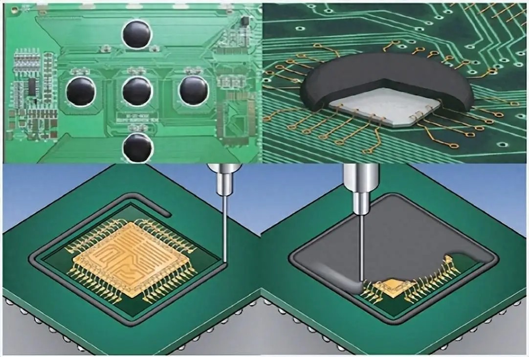
Figure 1. Underfill process
The underfill is a liquid encapsulant, usually an epoxy resin with a large amount of SiO2, which is used between the chip and the substrate after the flip chip interconnection. After curing, the hardened underfill has a high modulus, a low CTE that matches the solder joints, low moisture absorption, and good adhesion to the chip and substrate. The thermal stress on the solder joints is redistributed between the chip, underfill, substrate, and all solder joints, rather than concentrated on the peripheral solder joints. Application of underfill has been shown to reduce the most important solder joint strain level to 0.10-0.25 of the unpackaged solder joint strain. As a result, underfill can increase solder joint fatigue life by 10 to 100 times. In addition, it protects the solder joint from environmental corrosion. Underfill is a practical solution to expand the application of flip chip technology from ceramic substrates to organic substrates and from high-end products to cost-sensitive products.
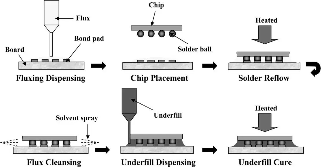
Figure 2. Flip chip process with underfill
Advances in flip chip technology have driven the development of underfill processes and underfill materials. Figure 2 shows the process steps of flip chip with underfill. Flux dispensing and cleaning steps are required before and after chip assembly. After the chip is assembled on the substrate, the unfilled material is dispensed and dragged into the gap between the chip and the substrate.
Foreign matter control before bottom filling glue application
Before applying the bottom filling glue, it is necessary to confirm that there are no foreign matter and a large amount of flux residue on the board surface and the filling surface. More flux residue will cause the adhesive to adhere to the flux residue. The volatilization, softening and variation of the flux residue in the subsequent use process will directly affect the mechanical properties of the adhesive, and then affect the reliability of the product. The standard bottom filling glue application process requires that the PCBA be cleaned and dried first, and then the glue is dispensed and cured.
The advantages of the bottom filling process are:
1. Improve the reliability of the solder joints and extend the service life of the product;
2. Protect the solder joints from environmental erosion and improve the corrosion resistance of the product;
3. Reduce the thermal stress between the chip and the substrate and improve the thermal cycle resistance of the product;
4. Enhance the adhesion between the chip and the substrate and improve the impact resistance and vibration resistance of the product.
Disadvantages of the bottom filling process:
1. Increase the cost and complexity of the package, and require additional equipment and materials;
2. It is necessary to select appropriate bottom filling materials and parameters to match the characteristics of the chip and substrate to avoid residual stress, cracks, corrosion, voids and other failure modes;
3. It is difficult to repair or rework the package, and the bottom filling needs to be removed to inspect or replace the solder joints;
4. It may affect the electrical performance of the chip, such as signal delay, crosstalk, noise, etc.


