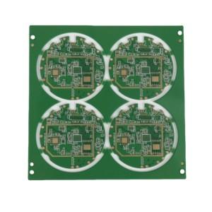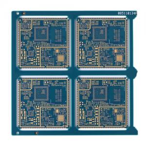
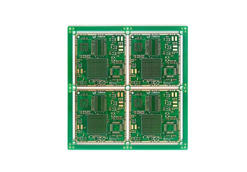
Description
The HDI board production process revolves around a sophisticated, layered methodology centered on "micro-via fabrication + sequential lamination." The standard workflow is divided into eight core stages, each subject to rigorous precision control requirements:
1. Preliminary Planning:PCB Design and Stack-up Planning
Engineers utilize EDA software to draft circuit schematics. Based on specific requirements, they plan the layer count, the placement of blind and buried vias, and the routing layout. By integrating Design for Manufacturability (DFM) principles early in the process—aligning the design with the factory's manufacturing capabilities during the initial phase—the risk of rework during subsequent prototyping is significantly reduced.
2. Inner Layer Circuit Fabrication
Laser drilling technology is employed to create pre-defined micro-vias on the inner core board. Subsequently, pattern transfer techniques are used to etch the circuit patterns onto the copper foil, thereby completing the formation of the inner layer circuitry. Throughout this entire process, strict control over precision and board surface cleanliness is maintained to prevent impurities from compromising the quality of the subsequent lamination.
3. Sequential Lamination (The Core HDI Process)
Unlike standard PCBs, which undergo a single, simultaneous lamination cycle, HDI boards are laminated in stages, layer by layer. Core boards containing the completed inner layer circuitry are stacked alternately with prepreg sheets (PP sheets). This stack is then cured under high temperature and high pressure within a vacuum laminator, progressively building a high-density interconnection network layer by layer. With each additional lamination cycle, the routing density increases correspondingly, and the HDI "order" (or complexity level) of the board advances.
4. Laser Drilling of Micro-vias
Laser drilling is the defining step that distinguishes HDI boards from standard PCBs. Addressing the requirement for micron-scale via diameters (typically ≤150 μm), laser technology is utilized to create the holes (CO₂ lasers are suitable for high-volume standard vias, while UV lasers are ideal for ultra-fine vias under 30 μm). This process is coupled with CCD visual positioning systems to ensure that via placement errors are confined to the micron level, thereby laying a solid foundation for reliable inter-layer connectivity.
5. Micro-via Plating and Filling
Through a pulsed plating process, copper is deposited uniformly onto the inner walls of the micro-vias. This process fills the blind vias, creating void-free conductive pathways. Upon completion of the filling process, Chemical Mechanical Polishing (CMP) is performed to ensure the board surface remains perfectly planar, providing an optimal foundation for the subsequent fabrication of the outer layers.
6. Outer Layer Circuit Fabrication
Grinding and cleaning processes are applied to remove any residual resin remaining after lamination. Laser drilling is then utilized once again to fabricate the outer-layer interconnect vias. An electroplating process is employed to establish conductive connections between the inner and outer layer circuitry, culminating in the final etching of the fine-pitch outer layer circuits in strict accordance with the design specifications. 7. Surface Finish
The appropriate surface finish process is selected based on the product's application requirements. Common options include OSP (Organic Solderability Preservative) and ENIG (Electroless Nickel Immersion Gold); the objective is to protect the copper surface while enhancing solderability and corrosion resistance.
8. Quality Inspection and Shipment
Depth-to-Diameter Ratio Paradox:The depth-to-diameter ratio of micro-vias in high-order HDI boards typically exceeds 2:1, making precise control of laser energy extremely difficult. Insufficient energy prevents the laser from drilling through the dielectric layer, whereas excessive energy risks burning through the underlying copper foil, thereby compromising the structural integrity and reliability of the board. 2. Difficulty in Controlling Cumulative Alignment Deviations Across Multiple Processing Cycles
High-density interconnect (HDI) boards of advanced orders require the repeated execution of a "laser drilling → plating → lamination" process sequence (an N-order board requires N rounds of laser drilling). Each processing cycle inevitably introduces errors:
The laminate material undergoes minute expansion and contraction following repeated high-temperature lamination cycles, causing cumulative errors to be progressively amplified. Consequently, the positional alignment accuracy for every drill hole must be controlled within ±10μm—a standard that traditional processing equipment struggles to meet consistently.
In stacked-via designs, subsequent drill holes must align precisely and coaxially with the underlying blind vias. An alignment deviation exceeding 5μm results in a "step" or offset, leading to defects in the via-filling plating process; as the HDI order increases, the product yield rate experiences a precipitous decline.
3. Stringent Requirements for Thermal Impact Control and Via Wall Quality
High-order HDI boards are predominantly utilized in high-frequency and high-speed applications, where the quality of the via walls directly dictates signal transmission performance:
Traditional CO₂ lasers employ a thermal processing mechanism, creating a heat-affected zone (HAZ) that can extend beyond 10μm. This often leads to carbonization of the via walls, decomposition of the resin, or even thermal burn-through of the adjacent dielectric layers. For high-order boards featuring thin dielectric layers (typically only a few tens of micrometers thick), this results in an extremely high finished-product scrap rate.
High-frequency applications mandate that via wall roughness be maintained below 0.5μm Ra. If the via walls are rough or uneven, it not only hinders the uniform deposition of the copper plating layer but also increases signal transmission loss, thereby triggering signal integrity issues.
4. Challenges in Adapting to Diverse Materials
To satisfy the demands of high-frequency and high-speed performance, high-order HDI boards frequently incorporate specialized substrate materials; however, the compatibility of these various materials with laser processing varies significantly:
High-frequency substrate materials—such as Polyimide (PI) and Liquid Crystal Polymer (LCP)—exhibit low absorption rates for infrared CO₂ lasers. Consequently, processing these materials requires significantly increased laser energy, which frequently induces material deformation. While UV lasers are capable of efficiently ablating and processing these materials, the capital cost of such equipment is more than double that of traditional systems.
Conversely, low-loss, high-speed substrate materials typically possess poor intrinsic thermal resistance. Even a marginally enlarged heat-affected zone can trigger delamination or blistering within the material, thereby imposing exceptionally rigorous requirements on the precision of thermal control during the laser processing stage. 5. Balancing Mass Production Yield and Cost Is Challenging
For high-end HDI, the yield rate for each individual laser drilling step must be maintained above 98%. After seven such processing steps, the cumulative overall yield stands at only approximately 87%. If the yield for a single step were to drop to 95%, the final yield would fall below 70%—a level entirely lacking in economic viability for mass production. Consequently, the demands placed on process control and equipment stability for high-end HDI are far more rigorous than those for standard HDI.
Material Compatibility Design: Dielectric thickness is selected based on laser processing capabilities, ensuring that the dielectric layer in a single lamination step does not exceed 120 μm; this prevents hole-wall defects caused by excessive aspect ratios during drilling. For specialized high-frequency substrates, material expansion and shrinkage compensation values are calculated and reserved in advance.
Routing Constraints: The spacing between micro-vias is maintained at no less than 0.15 mm to prevent carbonization of adjacent traces caused by the thermal impact of laser drilling; additionally, alignment targets are reserved to facilitate precise positioning and calibration via CCD systems.
2. Equipment and Process Controls: Stabilizing Yields at Every Stage
① Ensuring Long-Term Stability of Drilling Equipment
Laser focus and CCD positioning accuracy are calibrated regularly, and hole position deviations are verified weekly to ensure equipment deviation remains consistently within ±3 μm. Optical lenses and dust extraction systems are cleaned periodically to prevent airborne dust from compromising the uniformity of laser energy distribution.
A dual-laser collaborative process is employed: a UV laser is used to drill the copper foil, while a CO₂ laser drills the dielectric material. This clear division of labor not only ensures processing efficiency but also mitigates defects caused by over-processing associated with using a single laser source.
② Managing Material Expansion/Shrinkage and Alignment Deviations
Prior to drilling, PCB panels undergo a pre-baking treatment to release internal stresses and minimize subsequent expansion or shrinkage. The actual expansion/shrinkage coefficient for each batch of panels is measured empirically, and corresponding corrections are applied to the CAM data to offset dimensional changes resulting from the hot-pressing lamination process.
A "step-by-step" alignment strategy is adopted: after each lamination cycle, the panel's reference datum is re-established rather than relying solely on the initial datum. This approach prevents cumulative errors from exceeding acceptable tolerances after multiple rounds of processing. ③ Optimizing Drilling Processes to Minimize Intrinsic Defects
Laser parameters are adjusted according to the specific substrate material: for low-Dk, high-speed substrates, single-pulse energy is reduced, and a multi-scan drilling technique is employed to minimize thermal carbonization. For ultra-microvias smaller than 30μm, picosecond laser processing is utilized, which can reduce hole wall roughness by up to 60%.
Immediately following drilling, a plasma desmear process is performed to thoroughly remove carbonized residues from the hole walls, thereby preventing voids during electroplating and improving plating yield.
3. Closed-Loop, Layered Quality Control to Intercept Defects Early
First-Piece Comprehensive Inspection: For every new product model, the first piece produced undergoes a mandatory inspection comprising high-magnification microscopic analysis of hole walls, X-ray alignment verification, and probe-based hole diameter measurement. Mass production commences only after all parameters have been verified as compliant, thereby preventing batch-wide errors.
In-Process Patrol Inspection: Every two hours, a sampling inspection is conducted to verify drilling precision and hole wall quality; any detected deviations trigger immediate parameter adjustments to prevent the outflow of defective batches. Additionally, Automated Optical Inspection (AOI) is performed on all units to automatically identify visual defects, such as hole misalignment or missed holes.
Final Electrical Testing: All finished products undergo 100% electrical performance testing to screen for potential open circuits or short circuits within the microvias. This is combined with X-ray sampling inspections to verify the quality of internal via filling, ultimately ensuring a high shipment yield.
4. Data-Driven Traceability Management for Continuous Yield Optimization
An MES (Manufacturing Execution System) traceability system has been established, allowing for the tracking of process parameters for every board at every stage of production. In the event of a defect, the system enables rapid identification of the specific equipment or parameter responsible for the issue, facilitating continuous optimization of process parameters and a gradual improvement in mass production yields. Currently, leading manufacturers utilizing this comprehensive control methodology are able to consistently achieve mass production yields exceeding 90% for 3-tier HDI boards.
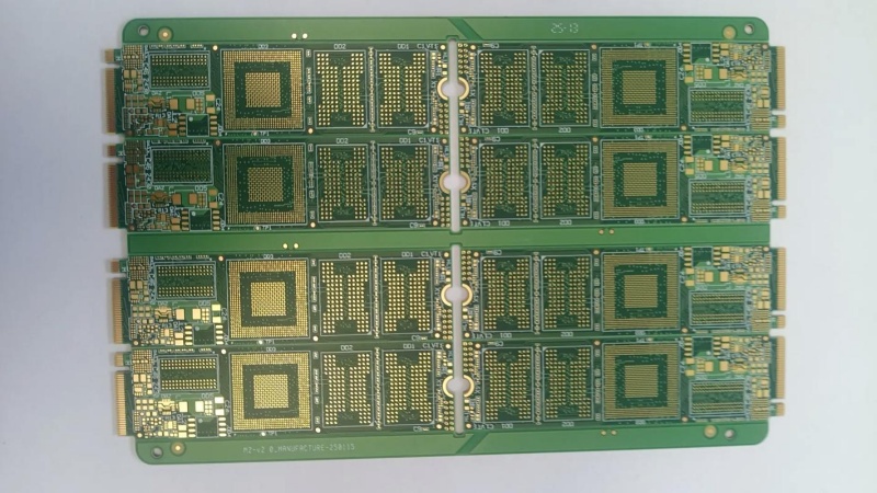
The five most common yield issues encountered during the mass production of high-end HDI PCBs, along with their corresponding rapid troubleshooting solutions, are summarized below:
1. Hole Position Misalignment → Excessive Cumulative Deviation
Typical Manifestation: Batch-produced blind vias are misaligned with inner-layer pads, resulting in open-circuit failures.
Rapid Troubleshooting Directions: ① Check if the PCB laminate underwent pre-baking to relieve internal stress; ② Check if the CCD camera lens is contaminated with dust, leading to inaccurate positioning; ③ Verify that expansion/shrinkage compensation was applied to each batch of laminates; ④ Check if the laser focal point has drifted.
2. Hole Wall Carbonization / Excessive Roughness
Typical Manifestation: Hole walls appear rough with black carbonized residue; voids are present within the filled vias after plating.
Rapid Troubleshooting Directions: ① Check if the laser power setting is too high; ② Verify that the correct laser type was selected (CO₂ lasers can easily cause carbonization when processing high-frequency substrates); ③ Confirm whether post-drilling plasma desmearing was performed; ④ Check if the dust extraction system is clogged, preventing the timely removal of debris.
3. Poor Via Filling / Excessive Plating Dimpling
Typical Manifestation: Voids are present within blind vias after filling; plating dimpling exceeds 10μm, compromising impedance consistency.
Rapid Troubleshooting Directions: ① Check if the laser drilling depth is consistent (excessive depth deviation leads to uneven copper filling); ② Check if the plating current parameters are optimized for deep-hole filling; ③ Verify that the chemical concentration in the plating bath is within normal limits; ④ For second-order stacked vias, confirm whether surface planarization (grinding) was performed after the first-stage via filling.
4. Inter-layer Misalignment / Delamination & Warpage
Typical Manifestation: Circuitry between layers is misaligned following multi-stage lamination; localized warpage exceeds specifications; delamination or "board blistering" occurs after thermal cycling.
Rapid Troubleshooting Directions:① Check if the lamination temperature and pressure profile complies with the laminate manufacturer's requirements, and if segmented temperature control was executed correctly; ② Verify that the inner-layer alignment CCD system has been properly calibrated; ③ Check if the resin flow characteristics of the prepreg material are compatible with the design requirements; ④ Confirm that the Coefficient of Thermal Expansion (CTE) of the PCB laminate meets the specific requirements for high-end HDI applications. 5. Excessive Impedance Deviation
Typical Manifestation: Batch-to-batch impedance fluctuations exceed tolerance limits, thereby compromising high-frequency signal transmission.
Rapid Troubleshooting Approaches: ① Verify whether copper thickness uniformity falls outside acceptable limits, as deviations in plating thickness can lead to impedance shifts; ② Confirm whether fluctuations in laser drilling depth are causing variations in the dielectric layer thickness; ③ Check if the lamination thickness tolerance exceeds ±0.05 mm; ④ Verify whether batch-to-batch variations in the substrate material's dielectric constant are excessive.
The five categories of issues listed above account for over 85% of defects encountered during the mass production of high-end HDI PCBs. By systematically following the troubleshooting sequence outlined above, the root cause can typically be identified within one hour, enabling rapid adjustments to restore yield rates.
1. Preliminary Planning:PCB Design and Stack-up Planning
Engineers utilize EDA software to draft circuit schematics. Based on specific requirements, they plan the layer count, the placement of blind and buried vias, and the routing layout. By integrating Design for Manufacturability (DFM) principles early in the process—aligning the design with the factory's manufacturing capabilities during the initial phase—the risk of rework during subsequent prototyping is significantly reduced.
2. Inner Layer Circuit Fabrication
Laser drilling technology is employed to create pre-defined micro-vias on the inner core board. Subsequently, pattern transfer techniques are used to etch the circuit patterns onto the copper foil, thereby completing the formation of the inner layer circuitry. Throughout this entire process, strict control over precision and board surface cleanliness is maintained to prevent impurities from compromising the quality of the subsequent lamination.
3. Sequential Lamination (The Core HDI Process)
Unlike standard PCBs, which undergo a single, simultaneous lamination cycle, HDI boards are laminated in stages, layer by layer. Core boards containing the completed inner layer circuitry are stacked alternately with prepreg sheets (PP sheets). This stack is then cured under high temperature and high pressure within a vacuum laminator, progressively building a high-density interconnection network layer by layer. With each additional lamination cycle, the routing density increases correspondingly, and the HDI "order" (or complexity level) of the board advances.
4. Laser Drilling of Micro-vias
Laser drilling is the defining step that distinguishes HDI boards from standard PCBs. Addressing the requirement for micron-scale via diameters (typically ≤150 μm), laser technology is utilized to create the holes (CO₂ lasers are suitable for high-volume standard vias, while UV lasers are ideal for ultra-fine vias under 30 μm). This process is coupled with CCD visual positioning systems to ensure that via placement errors are confined to the micron level, thereby laying a solid foundation for reliable inter-layer connectivity.
5. Micro-via Plating and Filling
Through a pulsed plating process, copper is deposited uniformly onto the inner walls of the micro-vias. This process fills the blind vias, creating void-free conductive pathways. Upon completion of the filling process, Chemical Mechanical Polishing (CMP) is performed to ensure the board surface remains perfectly planar, providing an optimal foundation for the subsequent fabrication of the outer layers.
6. Outer Layer Circuit Fabrication
Grinding and cleaning processes are applied to remove any residual resin remaining after lamination. Laser drilling is then utilized once again to fabricate the outer-layer interconnect vias. An electroplating process is employed to establish conductive connections between the inner and outer layer circuitry, culminating in the final etching of the fine-pitch outer layer circuits in strict accordance with the design specifications. 7. Surface Finish
The appropriate surface finish process is selected based on the product's application requirements. Common options include OSP (Organic Solderability Preservative) and ENIG (Electroless Nickel Immersion Gold); the objective is to protect the copper surface while enhancing solderability and corrosion resistance.
8. Quality Inspection and Shipment
Upon completion of the entire manufacturing process, the products undergo a multi-dimensional inspection sequence—including Automated Optical Inspection (AOI), X-Ray inspection, and flying-probe electrical testing—to verify the absence of issues such as circuit misalignment, micro-voids, or electrical faults. Once deemed compliant, the qualified products are cleaned, dried, packaged, and delivered.
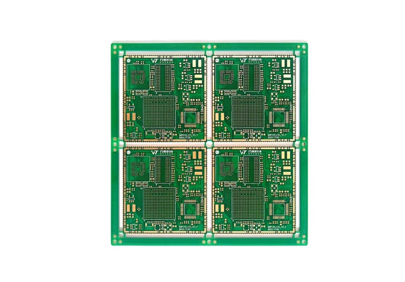
The laser drilling requirements for HDI boards of different orders vary significantly; as one progresses from first-order to second-order and then to higher orders, the demands for precision and process complexity increase progressively:
1. First-Order HDI Boards (Single Laser Drilling Pass)
Process Requirements: Only a single laser drilling pass is required. This involves processing a single-layer blind via connecting the surface layer to an adjacent inner layer; there is no need to account for interlayer alignment deviations.
Parameter Characteristics: The drilling depth is limited to the thickness of a single dielectric layer, and the aspect ratio (depth-to-diameter ratio) is typically ≤ 1:1. Standard CO₂ lasers are sufficient to meet these requirements, equipment precision demands are relatively low, and the yield rate can be consistently maintained above 98%.
Processing Challenges: The only significant challenge is controlling carbonization residues on the via walls; the process is mature and presents virtually no unique difficulties.
2. Second-Order HDI Boards (Double Laser Drilling Passes; Three Process Variations)
Second-order HDI boards feature three distinct design configurations, each imposing vastly different requirements on the laser drilling process:
① Staggered Via Design (Two Offset Drilling Passes)
This method requires two separate laser drilling passes: the first creates blind vias connecting Layer 1 (L1) to Layer 2 (L2); after lamination, a second pass creates blind vias connecting Layer 2 (L2) to Layer 3 (L3) at *offset positions*. Alignment error tolerances are strict (≤ ±15 μm), and it is necessary to compensate for the material expansion and contraction induced by the initial lamination process.
Essentially, this is equivalent to executing two separate first-order processes; consequently, the difficulty level is an order of magnitude higher than that of a standard first-order board. The final yield rate is the product of the yields from the two individual passes, resulting in a higher risk of cumulative material loss.
② Stacked Via Design (Two Vertically Aligned Drilling Passes)
This method requires two drilling passes executed at the *exact same vertical position*. The first blind via must be completely filled and planarized (leveled); otherwise, the second drilling pass may suffer from abnormal laser energy absorption or positional misalignment.
Alignment precision requirements are exceptionally stringent—demanding near-perfect vertical coincidence (error ≤ ±10 μm). This places extremely high demands on the laser's focusing precision and the CCD positioning system, making it the most technically challenging process among all second-order HDI configurations.
③ Skip Via Design (Single Pass Drilling Through to the Third Layer)
This method eliminates the need for two separate passes; instead, the laser drills directly from Layer 1 (L1) through to Layer 3 (L3) in a single operation. The drilling depth spans the thickness of two dielectric layers, and the aspect ratio can exceed 1.5:1. This process demands precise control over laser energy output: the beam must possess sufficient power to drill through both dielectric layers without damaging the copper foil on the third layer (L3), thereby imposing extremely rigorous requirements on the equipment's power control capabilities. Copper plating the hole walls also presents greater difficulty; the electroplating process must be optimized to ensure uniform copper thickness throughout the entire depth of the deep holes.
3. Third-Order and Higher-Order HDI Boards (Three or More Rounds of Laser Drilling)
These boards require three or more rounds of laser drilling combined with sequential lamination. Each step demands precise control over alignment errors; the cumulative error must be kept within ±20μm. Consequently, high-power UV lasers paired with high-precision CCD automatic alignment systems are mandatory.
The board material itself must possess an extremely low coefficient of thermal expansion. Otherwise, excessive expansion and contraction following multiple high-temperature lamination cycles will result in final hole position deviations that exceed acceptable limits.
Currently, only a select few leading manufacturers are capable of stably mass-producing third-order HDI boards with "any-layer interconnection" capabilities. The cost is 3 to 5 times that of first-order HDI boards, and they are primarily utilized in high-end flagship smartphones and core modules for AI servers.
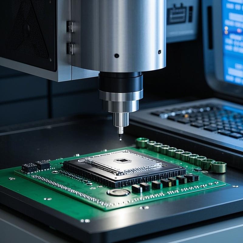
The core challenges associated with laser drilling for high-order HDI boards revolve around four main areas: ultra-small hole diameters, multi-round alignment precision, material compatibility, and hole wall quality. The specific difficulties are outlined below:
1. Ultra-Micro Hole Processing: Pushing the Limits of Dimensional Precision and Reliability
High-order HDI boards (such as sixth-order or "any-layer interconnection" designs) typically require micro-vias with diameters ranging from 50 to 75μm, while some high-end designs demand diameters as small as 30μm. Since these diameters are approximately half the size of those found in traditional HDI boards, the processing difficulty increases exponentially:
Depth-to-Diameter Ratio Paradox:The depth-to-diameter ratio of micro-vias in high-order HDI boards typically exceeds 2:1, making precise control of laser energy extremely difficult. Insufficient energy prevents the laser from drilling through the dielectric layer, whereas excessive energy risks burning through the underlying copper foil, thereby compromising the structural integrity and reliability of the board. 2. Difficulty in Controlling Cumulative Alignment Deviations Across Multiple Processing Cycles
High-density interconnect (HDI) boards of advanced orders require the repeated execution of a "laser drilling → plating → lamination" process sequence (an N-order board requires N rounds of laser drilling). Each processing cycle inevitably introduces errors:
The laminate material undergoes minute expansion and contraction following repeated high-temperature lamination cycles, causing cumulative errors to be progressively amplified. Consequently, the positional alignment accuracy for every drill hole must be controlled within ±10μm—a standard that traditional processing equipment struggles to meet consistently.
In stacked-via designs, subsequent drill holes must align precisely and coaxially with the underlying blind vias. An alignment deviation exceeding 5μm results in a "step" or offset, leading to defects in the via-filling plating process; as the HDI order increases, the product yield rate experiences a precipitous decline.
3. Stringent Requirements for Thermal Impact Control and Via Wall Quality
High-order HDI boards are predominantly utilized in high-frequency and high-speed applications, where the quality of the via walls directly dictates signal transmission performance:
Traditional CO₂ lasers employ a thermal processing mechanism, creating a heat-affected zone (HAZ) that can extend beyond 10μm. This often leads to carbonization of the via walls, decomposition of the resin, or even thermal burn-through of the adjacent dielectric layers. For high-order boards featuring thin dielectric layers (typically only a few tens of micrometers thick), this results in an extremely high finished-product scrap rate.
High-frequency applications mandate that via wall roughness be maintained below 0.5μm Ra. If the via walls are rough or uneven, it not only hinders the uniform deposition of the copper plating layer but also increases signal transmission loss, thereby triggering signal integrity issues.
4. Challenges in Adapting to Diverse Materials
To satisfy the demands of high-frequency and high-speed performance, high-order HDI boards frequently incorporate specialized substrate materials; however, the compatibility of these various materials with laser processing varies significantly:
High-frequency substrate materials—such as Polyimide (PI) and Liquid Crystal Polymer (LCP)—exhibit low absorption rates for infrared CO₂ lasers. Consequently, processing these materials requires significantly increased laser energy, which frequently induces material deformation. While UV lasers are capable of efficiently ablating and processing these materials, the capital cost of such equipment is more than double that of traditional systems.
Conversely, low-loss, high-speed substrate materials typically possess poor intrinsic thermal resistance. Even a marginally enlarged heat-affected zone can trigger delamination or blistering within the material, thereby imposing exceptionally rigorous requirements on the precision of thermal control during the laser processing stage. 5. Balancing Mass Production Yield and Cost Is Challenging
For high-end HDI, the yield rate for each individual laser drilling step must be maintained above 98%. After seven such processing steps, the cumulative overall yield stands at only approximately 87%. If the yield for a single step were to drop to 95%, the final yield would fall below 70%—a level entirely lacking in economic viability for mass production. Consequently, the demands placed on process control and equipment stability for high-end HDI are far more rigorous than those for standard HDI.
The core challenges in laser drilling for high-order HDI boards revolve around four key areas: ultra-small hole diameters, multi-cycle alignment precision, material compatibility, and hole wall quality. The specific difficulties are outlined below:
1. Ultra-Micro Hole Processing: The Ultimate Challenge in Dimensional Precision and Reliability
High-order HDI boards (such as 6-order or "Any-Layer Interconnect" designs) typically require micro-via diameters ranging from 50 to 75 μm; some high-end designs demand diameters as small as 30 μm—approximately half the size found in traditional HDI boards—resulting in an exponential increase in processing difficulty:
Physical Limits: Traditional laser spot sizes are often too large to be focused down to such ultra-fine diameters. UV lasers require integration with sub-micron-level optical systems to achieve the necessary beam shaping. Even a minuscule deviation in the laser spot position can lead to hole displacement or pad misalignment, ultimately resulting in open-circuit failures.
Aspect Ratio Challenges: The depth-to-diameter ratio of micro-vias in high-order HDI boards typically exceeds 2:1, making precise laser energy control extremely difficult. Insufficient energy prevents the laser from penetrating the dielectric layer, while excessive energy risks burning through the underlying copper foil, thereby compromising structural reliability.
2. Controlling Cumulative Alignment Deviations Across Multiple Processing Cycles
High-order HDI manufacturing necessitates multiple repetitions of the "laser drilling → plating → lamination" sequence (an N-order board requires N distinct laser drilling cycles). Each processing cycle introduces a certain degree of error:
The PCB substrate undergoes minute expansion and contraction during repeated high-temperature lamination cycles. These cumulative errors gradually amplify over time, requiring that the alignment precision for hole positioning be maintained within a strict tolerance of ±10 μm at every step—a standard that traditional processing equipment struggles to meet consistently.
In "stacked via" designs, subsequent drilling operations must achieve precise coaxial alignment with the underlying blind vias. An alignment error exceeding 5 μm creates a "step" or ledge within the hole, leading to defects during the via-filling plating process; consequently, the manufacturing yield rate suffers a precipitous decline as the number of stacked layers increases.
3. Stringent Requirements for Thermal Impact Control and Hole Wall Quality
High-order HDI boards are predominantly utilized in high-frequency and high-speed electronic applications, where the quality of the hole walls directly dictates signal transmission performance:
Traditional CO₂ lasers employ a thermal processing mechanism, resulting in a Heat-Affected Zone (HAZ) that can extend beyond 10 μm. This thermal exposure frequently triggers carbonization of the hole walls, decomposition of the resin dielectric, or even burn-through damage to adjacent dielectric layers. For high-order boards featuring ultra-thin dielectric layers (often merely a few tens of microns thick), these thermal effects lead to an extremely high rate of finished product rejection. High-frequency applications require the roughness of hole walls to be controlled below 0.5 μm Ra. If the hole walls are rough or uneven, it not only leads to non-uniform deposition of the electroplated copper layer but also increases signal transmission loss, thereby triggering signal integrity issues.
4. Challenges in Adapting to Diverse Materials
To meet the demands of high-frequency and high-speed performance, advanced HDI boards utilize a wide array of specialized substrate materials; however, the compatibility of these various materials with laser processing varies significantly:
High-frequency substrates—such as Polyimide (PI) and Liquid Crystal Polymer (LCP)—exhibit low absorption rates for infrared CO₂ lasers. Consequently, processing requires significantly increased laser energy, which frequently leads to material deformation. While UV lasers are capable of efficiently ablating these materials, the associated equipment costs are more than double those of other systems.
Low-loss, high-speed substrates inherently possess poor thermal resistance. Even a slightly enlarged heat-affected zone can result in delamination or blistering, thereby imposing extremely stringent requirements on the precision of thermal control during laser processing.
5. Balancing Mass Production Yields and Costs
For advanced HDI boards, the yield rate for each individual laser drilling step must be maintained above 98%. After undergoing seven such processing steps, the cumulative overall yield stands at only approximately 87%. Should the yield for a single step drop to 95%, the final cumulative yield would fall below 70%—a level that renders mass production economically unviable. Consequently, the demands placed on process control and equipment stability for advanced HDI manufacturing are far more rigorous than those for standard HDI boards.
Ensuring high mass-production yields for advanced HDI PCBs hinges on a three-pronged strategy: "proactive risk mitigation at the design stage," "comprehensive deviation control across the entire equipment and process workflow," and "closed-loop quality inspection to prevent escapes." Through precise control at multiple stages, yield losses are minimized to the lowest possible levels:
1. Front-loaded DFM (Design for Manufacturability) Reviews: Eliminating Mass-Production Risks in Advance
The root cause of many mass-production yield issues lies in flawed designs; early intervention through design reviews can reduce batch-level scrap rates by over 80%:
Material Compatibility Design: Dielectric thickness is selected based on laser processing capabilities, ensuring that the dielectric layer in a single lamination step does not exceed 120 μm; this prevents hole-wall defects caused by excessive aspect ratios during drilling. For specialized high-frequency substrates, material expansion and shrinkage compensation values are calculated and reserved in advance.
Routing Constraints: The spacing between micro-vias is maintained at no less than 0.15 mm to prevent carbonization of adjacent traces caused by the thermal impact of laser drilling; additionally, alignment targets are reserved to facilitate precise positioning and calibration via CCD systems.
2. Equipment and Process Controls: Stabilizing Yields at Every Stage
① Ensuring Long-Term Stability of Drilling Equipment
Laser focus and CCD positioning accuracy are calibrated regularly, and hole position deviations are verified weekly to ensure equipment deviation remains consistently within ±3 μm. Optical lenses and dust extraction systems are cleaned periodically to prevent airborne dust from compromising the uniformity of laser energy distribution.
A dual-laser collaborative process is employed: a UV laser is used to drill the copper foil, while a CO₂ laser drills the dielectric material. This clear division of labor not only ensures processing efficiency but also mitigates defects caused by over-processing associated with using a single laser source.
② Managing Material Expansion/Shrinkage and Alignment Deviations
Prior to drilling, PCB panels undergo a pre-baking treatment to release internal stresses and minimize subsequent expansion or shrinkage. The actual expansion/shrinkage coefficient for each batch of panels is measured empirically, and corresponding corrections are applied to the CAM data to offset dimensional changes resulting from the hot-pressing lamination process.
A "step-by-step" alignment strategy is adopted: after each lamination cycle, the panel's reference datum is re-established rather than relying solely on the initial datum. This approach prevents cumulative errors from exceeding acceptable tolerances after multiple rounds of processing. ③ Optimizing Drilling Processes to Minimize Intrinsic Defects
Laser parameters are adjusted according to the specific substrate material: for low-Dk, high-speed substrates, single-pulse energy is reduced, and a multi-scan drilling technique is employed to minimize thermal carbonization. For ultra-microvias smaller than 30μm, picosecond laser processing is utilized, which can reduce hole wall roughness by up to 60%.
Immediately following drilling, a plasma desmear process is performed to thoroughly remove carbonized residues from the hole walls, thereby preventing voids during electroplating and improving plating yield.
3. Closed-Loop, Layered Quality Control to Intercept Defects Early
First-Piece Comprehensive Inspection: For every new product model, the first piece produced undergoes a mandatory inspection comprising high-magnification microscopic analysis of hole walls, X-ray alignment verification, and probe-based hole diameter measurement. Mass production commences only after all parameters have been verified as compliant, thereby preventing batch-wide errors.
In-Process Patrol Inspection: Every two hours, a sampling inspection is conducted to verify drilling precision and hole wall quality; any detected deviations trigger immediate parameter adjustments to prevent the outflow of defective batches. Additionally, Automated Optical Inspection (AOI) is performed on all units to automatically identify visual defects, such as hole misalignment or missed holes.
Final Electrical Testing: All finished products undergo 100% electrical performance testing to screen for potential open circuits or short circuits within the microvias. This is combined with X-ray sampling inspections to verify the quality of internal via filling, ultimately ensuring a high shipment yield.
4. Data-Driven Traceability Management for Continuous Yield Optimization
An MES (Manufacturing Execution System) traceability system has been established, allowing for the tracking of process parameters for every board at every stage of production. In the event of a defect, the system enables rapid identification of the specific equipment or parameter responsible for the issue, facilitating continuous optimization of process parameters and a gradual improvement in mass production yields. Currently, leading manufacturers utilizing this comprehensive control methodology are able to consistently achieve mass production yields exceeding 90% for 3-tier HDI boards.
The five most common yield issues encountered during the mass production of high-end HDI PCBs, along with their corresponding rapid troubleshooting solutions, are summarized below:
1. Hole Position Misalignment → Excessive Cumulative Deviation
Typical Manifestation: Batch-produced blind vias are misaligned with inner-layer pads, resulting in open-circuit failures.
Rapid Troubleshooting Directions: ① Check if the PCB laminate underwent pre-baking to relieve internal stress; ② Check if the CCD camera lens is contaminated with dust, leading to inaccurate positioning; ③ Verify that expansion/shrinkage compensation was applied to each batch of laminates; ④ Check if the laser focal point has drifted.
2. Hole Wall Carbonization / Excessive Roughness
Typical Manifestation: Hole walls appear rough with black carbonized residue; voids are present within the filled vias after plating.
Rapid Troubleshooting Directions: ① Check if the laser power setting is too high; ② Verify that the correct laser type was selected (CO₂ lasers can easily cause carbonization when processing high-frequency substrates); ③ Confirm whether post-drilling plasma desmearing was performed; ④ Check if the dust extraction system is clogged, preventing the timely removal of debris.
3. Poor Via Filling / Excessive Plating Dimpling
Typical Manifestation: Voids are present within blind vias after filling; plating dimpling exceeds 10μm, compromising impedance consistency.
Rapid Troubleshooting Directions: ① Check if the laser drilling depth is consistent (excessive depth deviation leads to uneven copper filling); ② Check if the plating current parameters are optimized for deep-hole filling; ③ Verify that the chemical concentration in the plating bath is within normal limits; ④ For second-order stacked vias, confirm whether surface planarization (grinding) was performed after the first-stage via filling.
4. Inter-layer Misalignment / Delamination & Warpage
Typical Manifestation: Circuitry between layers is misaligned following multi-stage lamination; localized warpage exceeds specifications; delamination or "board blistering" occurs after thermal cycling.
Rapid Troubleshooting Directions:① Check if the lamination temperature and pressure profile complies with the laminate manufacturer's requirements, and if segmented temperature control was executed correctly; ② Verify that the inner-layer alignment CCD system has been properly calibrated; ③ Check if the resin flow characteristics of the prepreg material are compatible with the design requirements; ④ Confirm that the Coefficient of Thermal Expansion (CTE) of the PCB laminate meets the specific requirements for high-end HDI applications. 5. Excessive Impedance Deviation
Typical Manifestation: Batch-to-batch impedance fluctuations exceed tolerance limits, thereby compromising high-frequency signal transmission.
Rapid Troubleshooting Approaches: ① Verify whether copper thickness uniformity falls outside acceptable limits, as deviations in plating thickness can lead to impedance shifts; ② Confirm whether fluctuations in laser drilling depth are causing variations in the dielectric layer thickness; ③ Check if the lamination thickness tolerance exceeds ±0.05 mm; ④ Verify whether batch-to-batch variations in the substrate material's dielectric constant are excessive.
The five categories of issues listed above account for over 85% of defects encountered during the mass production of high-end HDI PCBs. By systematically following the troubleshooting sequence outlined above, the root cause can typically be identified within one hour, enabling rapid adjustments to restore yield rates.