Description
With the development of electronic devices towards high frequency, high speed, and high density, high-density interconnect (HDI) boards are becoming increasingly widely used in smartphones, 5G communication equipment, automotive electronics, and other fields. In these applications, the integrity and stability of signal transmission are crucial, and impedance control technology is key to ensuring high-speed signal transmission.

High-density routing: The trace width and spacing of HDI boards are small, which can easily lead to impedance fluctuations.
Multi-layer structure: The complex stacking structure and micro-via technology increase the difficulty of impedance control.
High-frequency signals: In high-frequency applications, signals are more sensitive to impedance changes, requiring higher design precision.
Material characteristics: The dielectric constant (Dk) and loss factor (Df) of different materials affect the stability of the impedance.
Key Technologies for High-Density Interconnect Board Impedance Control
To achieve precise impedance control, HDI board design needs to address the following aspects:
Trace spacing: In high-density routing, excessively small trace spacing can lead to crosstalk; reasonable spacing design is needed to reduce interference.
Reference plane: The reference plane below or above the traces (usually a ground plane or power plane) is crucial for impedance control. Ensure the integrity and continuity of the reference plane.
Loss Factor (Df): Materials with a low loss factor help improve signal transmission efficiency.
Consistency: Ensure that the dielectric constant and thickness of the materials remain consistent during the manufacturing process to avoid impedance fluctuations.
Blind and Buried Vias: Reasonably design blind and buried vias to avoid interference with trace impedance.
Test Verification: Verify the impedance of the finished board using test equipment such as time-domain reflectometers (TDR) to ensure consistency with the design values.
HDI PCB impedance control technology is crucial for ensuring high-speed signal transmission and directly affects the performance and reliability of electronic devices. By optimizing trace design, layered structure, material selection, and manufacturing processes, precise impedance control can be achieved to meet the needs of high-frequency and high-speed applications.
As a leading supplier of HDI board technology, KEY TECHNOLOGY is committed to providing customers with high-performance, high-reliability solutions. If you encounter challenges in impedance control in your HDI board design, please feel free to contact our technical team. We will provide you with professional support and services.
What is impedance control?
Impedance control refers to the technology used in PCB design to precisely control the geometric shape of the traces, material characteristics, and interlayer structure to match the impedance of the signal transmission line with the characteristic impedance of the system, thereby reducing signal reflection and loss and ensuring signal integrity.
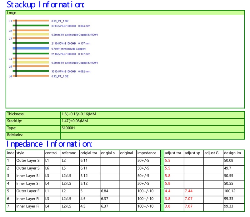
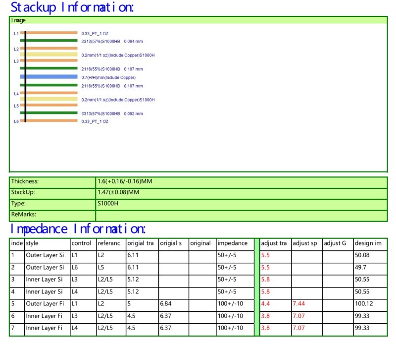
In high-speed signal transmission, impedance mismatch can lead to signal reflection, crosstalk, and attenuation, which in turn affects the performance of the device. Therefore, impedance control is a core aspect of HDI board design.

Challenges of HDI Board Impedance Control
High-density routing: The trace width and spacing of HDI boards are small, which can easily lead to impedance fluctuations.
Multi-layer structure: The complex stacking structure and micro-via technology increase the difficulty of impedance control.
High-frequency signals: In high-frequency applications, signals are more sensitive to impedance changes, requiring higher design precision.
Material characteristics: The dielectric constant (Dk) and loss factor (Df) of different materials affect the stability of the impedance.
Key Technologies for High-Density Interconnect Board Impedance Control
To achieve precise impedance control, HDI board design needs to address the following aspects:
(1) Trace Design Optimization
Trace width and thickness: The width and copper foil thickness of the traces directly affect the impedance value. Appropriate trace dimensions are determined through precise calculations and simulations.Trace spacing: In high-density routing, excessively small trace spacing can lead to crosstalk; reasonable spacing design is needed to reduce interference.
Reference plane: The reference plane below or above the traces (usually a ground plane or power plane) is crucial for impedance control. Ensure the integrity and continuity of the reference plane.
(2) Layer Stackup Design
Dielectric layer thickness: The thickness of the dielectric layer directly affects the distance between the traces and the reference plane, thus affecting the impedance value. Precise control of the dielectric layer thickness is ensured through optimization of the layer stackup. Symmetrical Design: Using a symmetrical layered structure can reduce impedance fluctuations and improve signal transmission stability.
(3) Material Selection
Dielectric Constant (Dk): Choosing materials with a low dielectric constant can reduce signal delay and loss.Loss Factor (Df): Materials with a low loss factor help improve signal transmission efficiency.
Consistency: Ensure that the dielectric constant and thickness of the materials remain consistent during the manufacturing process to avoid impedance fluctuations.
(4) Microvia and Blind Via Design
Microvia Technology: The microvia technology widely used in HDI boards places higher demands on impedance control. Optimize the size and location of microvias to reduce their impact on signal transmission.Blind and Buried Vias: Reasonably design blind and buried vias to avoid interference with trace impedance.
(5) Simulation and Testing
Simulation Tools: Use professional PCB simulation tools (such as SI9000, HyperLynx, etc.) for impedance simulation to ensure that the design meets the requirements.Test Verification: Verify the impedance of the finished board using test equipment such as time-domain reflectometers (TDR) to ensure consistency with the design values.
HDI PCB impedance control technology is crucial for ensuring high-speed signal transmission and directly affects the performance and reliability of electronic devices. By optimizing trace design, layered structure, material selection, and manufacturing processes, precise impedance control can be achieved to meet the needs of high-frequency and high-speed applications.
As a leading supplier of HDI board technology, KEY TECHNOLOGY is committed to providing customers with high-performance, high-reliability solutions. If you encounter challenges in impedance control in your HDI board design, please feel free to contact our technical team. We will provide you with professional support and services.
