KEY TECHNOLOGY(HK)CO. ,LIMITED
  • Home
  • Products
    • PCBA
    • Rigid PCB
    • HDI PCB
    • Rigid Flex PCB
    • Flex PCB
    • High Frequency PCB
      • Rogers PCB
      • Isola PCB
      • Arlon PCB
      • Nelco PCB
      • Taconic PCB
      • Teflon PCB
      • Neltec PCB
    • Metal Core PCB
      • Aluminium PCB
      • Copper PCB
    • Ceramic PCB
    • Laser Stencil
    • Reverse engineering
    • Purchasing components
  • Capability
    • PCBA capability
    • Rigid PCB capability
    • HDI PCB Capability
    • Rigid Flex PCB Capability
    • Flex PCB Capability
    • High Frequency PCB Capability
    • Metal Core PCB Capability
    • Ceramic PCB Capability
  • Equipment
    • PCB Equipment
    • PCBA Equipment
  • About us
  • Blogs
  • Feedback
  • Contact us
  1. Home
  2. Products
  3. Rigid PCB
  4. Gold finger PCB
  • Gold finger PCB
  • Gold finger PCB
  • Gold finger PCB
PrevNext

Gold finger PCB

  • Product Item:KEY Gold finger PCB-04
  • Gold finger PCB
  • TG:170
  • ENIG
  • IPC ClassIII
  • Gold finger PCB  , FR-4  , IPC CLASSIII  , ENIG  , green soldermask  , white silkscreen  , immersion gold  , tg170
    Inquiry Send Email PDF

    Description

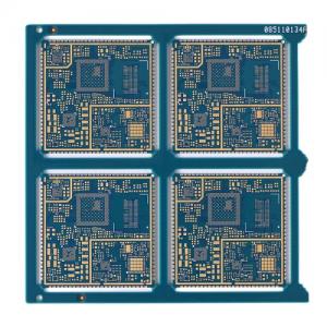
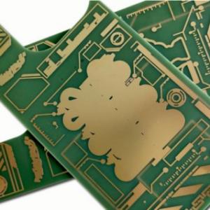
    This is rigid PCB,

    Gold finger PCB

    material is FR-4 with green soldermask,

    surface treatment ENIG (immersion gold) ,

    high TG 170, IPC class III,

    1oz copper thick,

    1.6mm board thick

    min hole 0.3mm

    min trace width/min distance 12mil

    Gold finger PCB is a kind of commonly used circuit board in the PCB design and manufacturing industry, also known as Edge Connector. Its role is as the export of the external connection network of the board, and the connection with other devices is achieved through the plugging of the connector. The gold finger usually consists of a row of golden conductive contact pieces, and the shape and arrangement of these contact pieces are similar to fingers, hence the name.

    The surface treatment methods of gold finger PCB mainly include electroplating nickel and gold and immersion gold. Electroplating nickel and gold has superior conductivity, oxidation resistance and wear resistance, and is often used in PCB boards that need frequent plugging or mechanical friction. Immersion gold has good conductivity, flatness and solderability, and is suitable for high-precision PCB boards with designs such as key positions, bonded ICs, BGA, etc.

    In PCB design, the detailed treatment of gold fingers is also very important. In order to increase the wear resistance of the gold finger, hard gold plating is usually required. The gold finger also needs to be chamfered, generally 45°, and other angles such as 20° and 30° are also possible. In addition, the gold finger needs to do the whole solder mask opening treatment, and the PIN does not need to open the stencil. The solder-tin and solder-silver pads need to have a minimum distance of 14 mil from the top of the finger, and it is recommended that when designing, the pad be more than 1mm away from the finger position, including the via pad. There should be no copper plating on the surface layer of the gold finger, and all inner layers need to do copper reduction treatment. Usually, the copper reduction width is more than 3mm, and half-finger copper reduction and whole-finger copper reduction can be done.

    Inquiry Us


    Related Products

    ceramic PCB

    ceramic PCB

    Al2O3 ceramic PCB

    Al2O3 ceramic PCB

    HDI PCB Manufacturer-High Density Interconnect PCB

    HDI PCB Manufacturer-High Density Interconnect PCB

    How to choose a PCBA Manufacturing factory

    How to choose a PCBA Manufacturing factory

    Rogers RT/Duriod 6035 PCB

    Rogers RT/Duriod 6035 PCB

    PCB ASSEMBLY FACTORY

    PCB ASSEMBLY FACTORY

    Product Categories

    • PCBA
    • Rigid PCB
    • HDI PCB
    • Rigid Flex PCB
    • Flex PCB
    • High Frequency PCB
      • Rogers PCB
      • Isola PCB
      • Arlon PCB
      • Nelco PCB
      • Taconic PCB
      • Teflon PCB
      • Neltec PCB
    • Metal Core PCB
      • Aluminium PCB
      • Copper PCB
    • Ceramic PCB
    • Laser Stencil
    • Reverse engineering
    • Purchasing components

    Links

    Google.comBaidu.com

    内页左侧广告1

    Feedback

    Contact Us

    sales@key-pcba.com

    234123644@qq.com

    Commercial and Cultural Building, Community 11 of Tangwei,Fuhai Street, Bao'An District Shenzhen 518103 GuangDong China.

    WECHAT

    Copyright © 2016 KEY TECHNOLOGY(HK)CO. ,LIMITED All Rights Reserved.

    • Skype.
    • E-mail
    • Whatsapp
    • Inquiry