Electrical clearance and creepage distance details and handling in PCB
In the high-voltage PCB design is also a switching power supply PCB design is more important to determine the electrical gap and creepage distance, if the electrical gap and creepage distance is too small, you need to pay attention to the leakage of a situation.Definition of creepage spacing and electrical clearance
Electrical clearance: the shortest space between the conductive parts of the distance.
Creepage distance: the shortest distance between conductive parts along the surface of the insulating material.
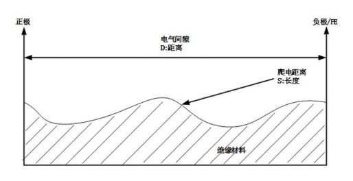
Electrical clearance, creepage distance illustration
In the design of high-voltage PCB process, many students can not grasp the value of the electrical gap and creepage distance, of course, the value of the electrical gap and creepage distance is not empty, is required to determine a series of parameters, including insulation type, insulation materials, overvoltage and pollution level of such parameters to determine the factors.
Among them, the level of insulation type is introduced
◆ Functional insulation: insulation between conductive parts, and only to ensure the normal operation of the system.
◆ Basic insulation: insulation between conductive parts, used to prevent lightning strikes.
◆ Supplementary insulation: A type of insulation other than basic insulation, which is used to further prevent the click if the basic insulation fails.
◆ Double insulation: The combination of basic insulation and supplementary insulation.
◆ Enhanced insulation: A single insulation system that provides protection against clicking by determining the relevant criteria, equivalent to double insulation.
◆ Safety insulation: The distance of guiding electric parts, including double insulation or reinforced insulation.
Insulation material grade introduction
◆ Material group 1: CTI≥600
◆ Material group 2: 400≤CTI<400
◆ Material group 3a:175≤CTI<400
◆ Material group 3b:100≤CTI<170
CTI: relative leakage start index, the material surface can withstand 50 drops of electrolyte (0.1% aqueous ammonia chloride solution) and the formation of leakage traces of the highest voltage value in V.
Switching power supply material group usually according to material group 3a, a few in material group 2, high-voltage module is generally material group 1.
Overvoltage level introduction
◆ Overvoltage class 1: Systems that are connected to the power supply only and have taken measures to limit voltage surges so that the surge voltage is sufficiently low.
◆ Overvoltage class 2: applied to systems connected to a fixed power source, including household equipment and portable devices.
Overvoltage class 3: Used in systems connected to a fixed power supply, but with special requirements for reliability and availability, such as industrial systems
Overvoltage class 4: Used in field power supply systems such as those connected to electric meters
Switching power supplies are usually rated according to overvoltage class 2 (e.g. for consumer products) and, to a lesser extent, overvoltage class 3 (e.g. for industrial applications).
Pollution class introduction
◆ Contamination level 1: No or only dry non-conductive contaminants are present, and they have no effect on the operation of the system.
◆ Contamination class 2: Under normal conditions, only non-conductive contaminants appear. If the component is not in operating condition, dew will cause slight conductivity.
◆ Pollution level 3: conductive contaminants are allowed to appear, for example, when dew occurs, conductive through dry, non-conductive contaminants under normal conditions.
◆ Pollution level 4: Allow the appearance of continuous pollutants, such as conductive dust, rain and snow.
◆ Switching power supply: usually according to pollution level 2, very few according to pollution level 3.
Suppose the current system voltage is 220V this time you can go to the table, through the following table can be derived from the pulse voltage (Impulse voltage) this value, as well as the overvoltage level (through the previous description can be derived, switching power supply overvoltage level recommended overvoltage level 2)
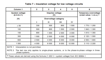
Then, based on the known system voltage value and overvoltage value, we can get the pulse voltage value of 2500 V. Looking at the table below, we can directly get the electrical gap.
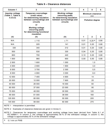
The value of electrical clearance can be directly derived from the above table as 1.5mm.
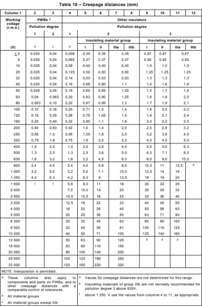
The same is true for the creepage distance, which is shown in the table below. Before determining the creepage distance, it is necessary to know the operating voltage and the pollution level and insulation material group mentioned above, and to confirm the creepage distance in the high-voltage design according to these values. Suppose the current operating voltage is 220V, through the previous article can know the common pollution level and high voltage module material group in the switching power supply and consumer boards, generally refer to the pollution level 2 and insulation material group 3a, and then through the following table to find the value of the creepage distance can be derived from 2.5mm.
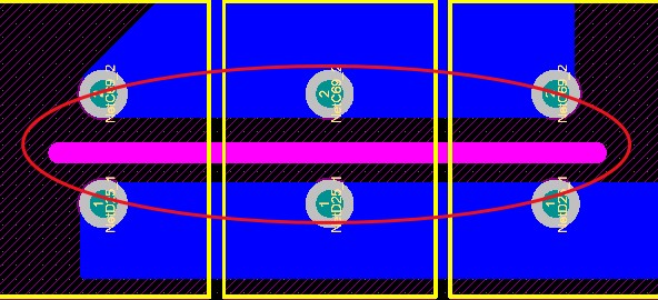
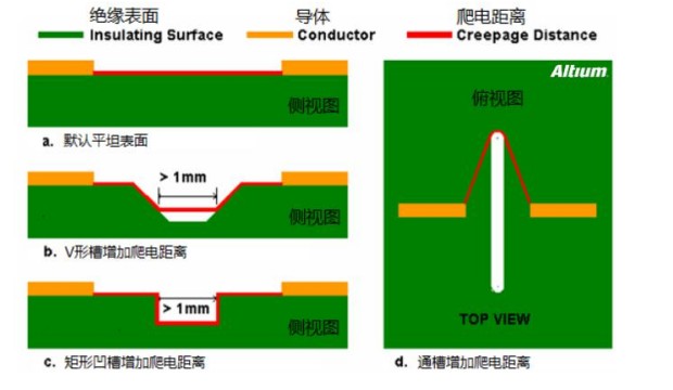
Through the above introduction of the basic can probably understand the creepage spacing and electrical gap, that in the PCB how to deal with it, you can see the following whole picture, the spacing of the electrical gap and then the layout of the PCB to adjust the device pad to pad spacing, and creepage spacing sometimes if the space on the PCB board is relatively tight when you can increase the creepage spacing by digging a slot.
The design method in the PCB
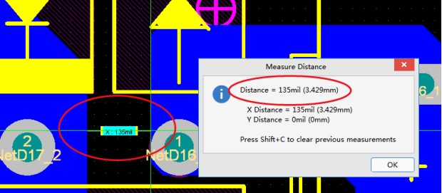
The following figure is a creepage spacing of 220V, so that the creepage spacing is guaranteed to be greater than 2.5mm.
If some places are encountered where the creepage spacing cannot be met, slotting can be done. The width of its slotting meets a minimum width of 1mm. Prevent the risk of electricity leakage.