KEY TECHNOLOGY(HK)CO. ,LIMITED
  • Home
  • Products
    • PCBA
    • Rigid PCB
    • HDI PCB
    • Rigid Flex PCB
    • Flex PCB
    • High Frequency PCB
      • Rogers PCB
      • Isola PCB
      • Arlon PCB
      • Nelco PCB
      • Taconic PCB
      • Teflon PCB
      • Neltec PCB
    • Metal Core PCB
      • Aluminium PCB
      • Copper PCB
    • Ceramic PCB
    • Laser Stencil
    • Reverse engineering
    • Purchasing components
  • Capability
    • PCBA capability
    • Rigid PCB capability
    • HDI PCB Capability
    • Rigid Flex PCB Capability
    • Flex PCB Capability
    • High Frequency PCB Capability
    • Metal Core PCB Capability
    • Ceramic PCB Capability
  • Equipment
    • PCB Equipment
    • PCBA Equipment
  • About us
  • Blogs
  • Feedback
  • Contact us
  1. Home
  2. Products
  3. HDI PCB
  4. 2 step HDI PCB
  • 2 step HDI PCB

2 step HDI PCB

  • Product Item:KEY HDI-01
  • 2step
  • Buried blind hole
  • 3R+6F+3R
  • BGA
  • 12layer  , 2step HDI  , buried blind hole PCB  , 3R+6F+3R
    Inquiry Send Email

    Description

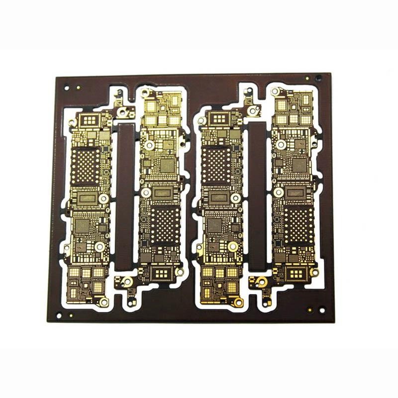
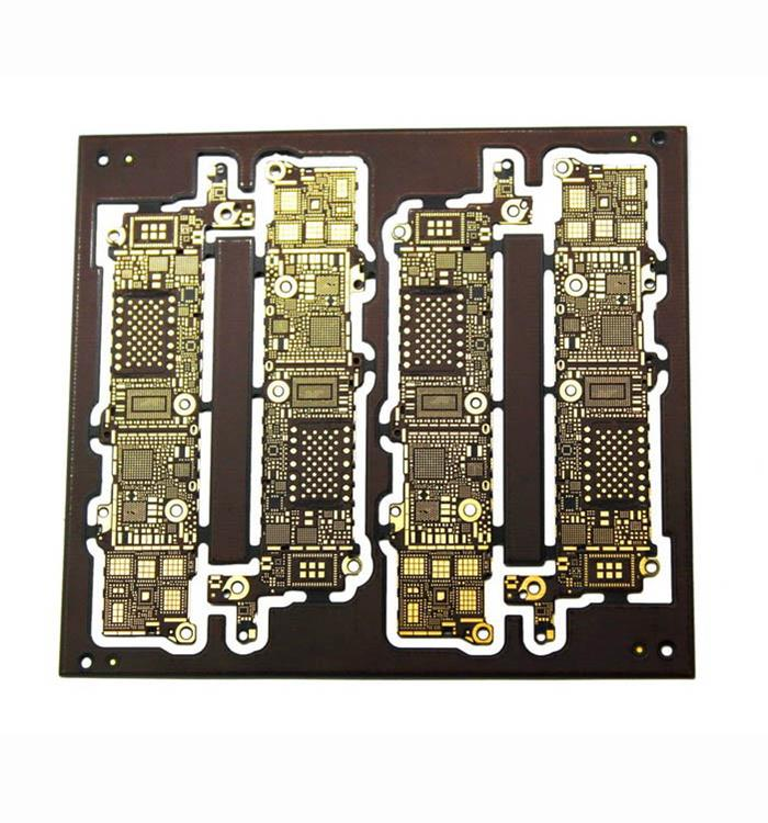
    12 layer 2step HDI high-precision buried blind hole HDI PCB

    Layers: 12

    PCB board thick: 2.0 ± 0.15 mm

    Plate used: FR4 ShengYi
    Minimum hole diameter: 0.1mm
    Surface treatment: ENIG
    BGA size: 0.25mm
    Minimum trace width/distance: 0.13mm/0.15mm
    Blind hole structure: 3R+6F+3R (12 layer 2step HDI)
    Process characteristics: HDI blind hole process, high BGA density, small spacing between hole to trace
    Application field: high-end digital camera

    A 2-stage HDI PCB refers to a multilayer printed circuit board (PCB) manufactured using High-Density Interconnect (HDI) technology. It is characterized by the use of micro-blind vias and buried vias for interlayer connection inside the PCB, thereby improving the wiring density and performance of the PCB.

    The manufacturing process of a 2-stage HDI PCB generally includes the following steps:

    1. Inner layer circuit fabrication: Form copper foil circuit patterns on the inner substrate.
    2. Lamination: Bond the inner substrate with the outer substrate together through the lamination process.
    3. Drilling: Use laser drilling technology to drill holes on the PCB, including blind vias and buried vias.
    4. Copper plating: Copper plating is performed in the drilled holes to increase conductivity.
    5. Outer layer circuit fabrication: Form copper foil circuit patterns on the outer layer of the PCB.
    6. Surface treatment: Perform surface treatment on the PCB, such as solder mask and silk screen printing.

    A 2-stage HDI PCB has higher density, better performance and smaller size compared to traditional PCBs. It is often used in high-end electronic products such as mobile phones, tablet computers, and notebook computers.

    Inquiry Us


    Related Products

    How to select a reliable PCBA manufacturer in China?

    How to select a reliable PCBA manufacturer in China?

    PCB gold finger connector

    PCB gold finger connector

    LED PCB Conclusion

    LED PCB Conclusion

    Computer motherboard PCBA

    Computer motherboard PCBA

    Rogers 3006

    Rogers 3006

    RT/duroid 5880

    RT/duroid 5880

    Product Categories

    • PCBA
    • Rigid PCB
    • HDI PCB
    • Rigid Flex PCB
    • Flex PCB
    • High Frequency PCB
      • Rogers PCB
      • Isola PCB
      • Arlon PCB
      • Nelco PCB
      • Taconic PCB
      • Teflon PCB
      • Neltec PCB
    • Metal Core PCB
      • Aluminium PCB
      • Copper PCB
    • Ceramic PCB
    • Laser Stencil
    • Reverse engineering
    • Purchasing components

    Links

    Google.comBaidu.com

    内页左侧广告1

    Feedback

    Contact Us

    sales@key-pcba.com

    234123644@qq.com

    Commercial and Cultural Building, Community 11 of Tangwei,Fuhai Street, Bao'An District Shenzhen 518103 GuangDong China.

    WECHAT

    Copyright © 2016 KEY TECHNOLOGY(HK)CO. ,LIMITED All Rights Reserved.

    • Skype.
    • E-mail
    • Whatsapp
    • Inquiry