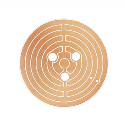
KEY TECHNOLOGY(HK)CO. ,LIMITED
  • Home
  • Products
    • PCBA
    • Rigid PCB
    • HDI PCB
    • Rigid Flex PCB
    • Flex PCB
    • High Frequency PCB
      • Rogers PCB
      • Isola PCB
      • Arlon PCB
      • Nelco PCB
      • Taconic PCB
      • Teflon PCB
      • Neltec PCB
    • Metal Core PCB
      • Aluminium PCB
      • Copper PCB
    • Ceramic PCB
    • Laser Stencil
    • Reverse engineering
    • Purchasing components
  • Capability
    • PCBA capability
    • Rigid PCB capability
    • HDI PCB Capability
    • Rigid Flex PCB Capability
    • Flex PCB Capability
    • High Frequency PCB Capability
    • Metal Core PCB Capability
    • Ceramic PCB Capability
  • Equipment
    • PCB Equipment
    • PCBA Equipment
  • About us
  • Blogs
  • Inquiry
  • Contact us
  1. Home
  2. Products
  3. Ceramic PCB
  4. ceramic PCB
  • ceramic PCB

ceramic PCB

  • Product Item:key ceramic-02
  • ceramic
  • 96% Al2O3
  • 30w
  • 3u
  • Al2O3 ceramic PCB  , Thermal conductivity 35w  , 96AL2O3
    Inquiry Send Email

    Description

    Al2O3 ceramic PCB,

    layers 1-layer,

    board thick 0.8+/-0.1mm,

    plate 96%AL2O3,

    min hole 0.8mm,

    surface finish ENIG,

    Thermal conductivity of insulation layer 30W,

    out layer copper thick:70um,

    Au >=3u"

    technology charactors: through hole, dpc technology

    Request CERAMIC PCB Quote Now
    The manufacturing process of aluminum oxide ceramic PCB mainly includes single-sintering multi-layer method and thick film multi-layer method. The simple process flows of these two methods are as follows:

    I. Single-sintering multi-layer method:
    1. Stamping of ceramic blank;
    2. Printing of conductive layer;
    3. Laminating or printing of insulation layer;
    4. Blanking of external shape;
    5. Sintering;
    6. Plating of precious metals.

    Request CERAMIC PCB Quote Now

    II. Thick film multi-layer method:
    1. Stamping of ceramic blank;
    2. Sintering;
    3. Printing of conductive layer;
    4. Sintering;
    5. Printing of insulation layer;
    6. Printing of conductive layer;
    7. Sintering (operating back and forth according to the number of layers).

    Inquiry Us


    Related Products

    Arlon high frequency PCB

    Arlon high frequency PCB

    COPPER PCB

    COPPER PCB

    Blind via hole in PCB design layout

    Blind via hole in PCB design layout

    Rogers RT/Duriod 6035 PCB

    Rogers RT/Duriod 6035 PCB

    PCB Blind via vs microvia

    PCB Blind via vs microvia

    Prototype PCB assembly

    Prototype PCB assembly

    Product Categories

    • PCBA
    • Rigid PCB
    • HDI PCB
    • Rigid Flex PCB
    • Flex PCB
    • High Frequency PCB
      • Rogers PCB
      • Isola PCB
      • Arlon PCB
      • Nelco PCB
      • Taconic PCB
      • Teflon PCB
      • Neltec PCB
    • Metal Core PCB
      • Aluminium PCB
      • Copper PCB
    • Ceramic PCB
    • Laser Stencil
    • Reverse engineering
    • Purchasing components

    Links

    Google.comBaidu.com

    内页左侧广告1

    Feedback

    Contact Us

    sales@key-pcba.com

    234123644@qq.com

    Commercial and Cultural Building, Community 11 of Tangwei,Fuhai Street, Bao'An District Shenzhen 518103 GuangDong China.

    WECHAT

    Copyright © 2016 KEY TECHNOLOGY(HK)CO. ,LIMITED All Rights Reserved.

    • Skype.
    • E-mail
    • Whatsapp
    • Inquiry