KEY TECHNOLOGY(HK)CO. ,LIMITED
  • Home
  • Products
    • PCBA
    • Rigid PCB
    • HDI PCB
    • Rigid Flex PCB
    • Flex PCB
    • High Frequency PCB
      • Rogers PCB
      • Isola PCB
      • Arlon PCB
      • Nelco PCB
      • Taconic PCB
      • Teflon PCB
      • Neltec PCB
    • Metal Core PCB
      • Aluminium PCB
      • Copper PCB
    • Ceramic PCB
    • Laser Stencil
    • Reverse engineering
    • Purchasing components
  • Capability
    • PCBA capability
    • Rigid PCB capability
    • HDI PCB Capability
    • Rigid Flex PCB Capability
    • Flex PCB Capability
    • High Frequency PCB Capability
    • Metal Core PCB Capability
    • Ceramic PCB Capability
  • Equipment
    • PCB Equipment
    • PCBA Equipment
  • About us
  • Blogs
  • Inquiry
  • Contact us
  1. Home
  2. Products
  3. PCBA Manufacturing Process Analysis
  • PCBA Manufacturing Process Analysis
  • PCBA Manufacturing Process Analysis
  • PCBA Manufacturing Process Analysis
PCBA Manufacturing Process Analysis PCBA Manufacturing Process Analysis PCBA Manufacturing Process Analysis

PCBA Manufacturing Process Analysis

  • Product Item:KEY-PCBA 82
  • PCBA Manufacturing Process Analysis
  • PCBA Manufacturing
  • PCBA Analysis
  • PCBA Process Analysis
  • Inquiry Send Email

    Description

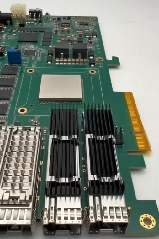
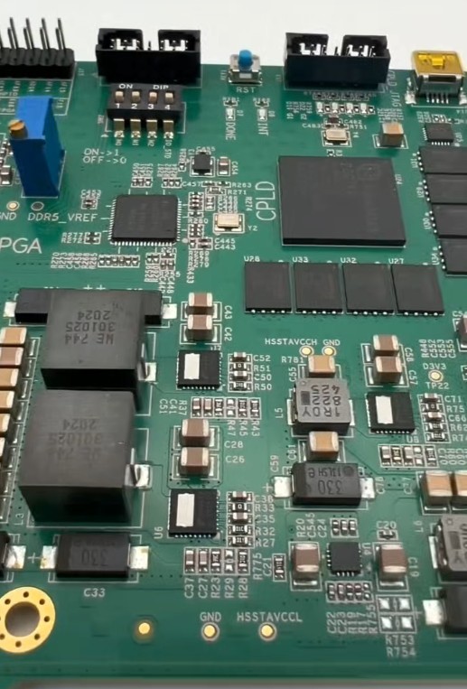
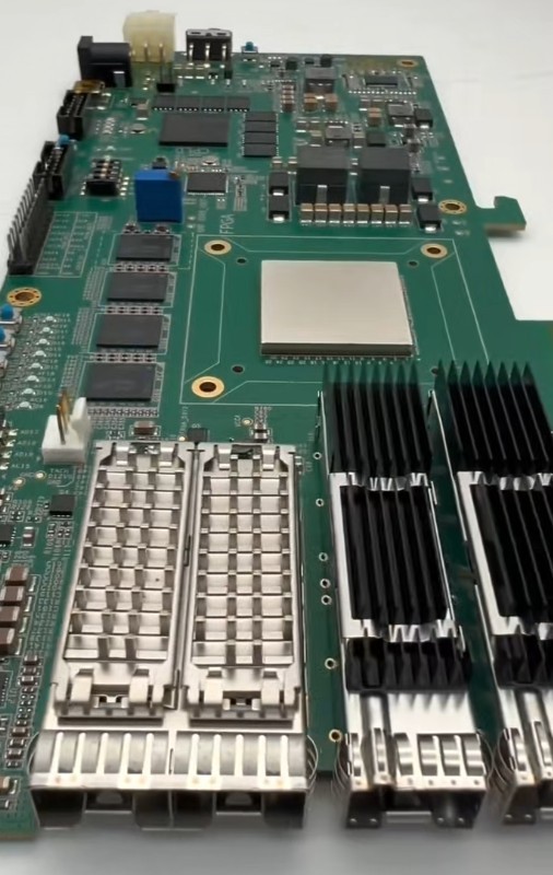
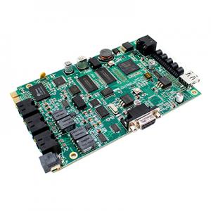
    PCBA stands for Printed Circuit Board Assembly. A PCBA consists of a PCB (Printed Circuit Board) and connected electronic components. This article breaks down the structure, manufacturing process shares the information with you.

    I. PCBA Structure Analysis

    PCBA consists of a bare PCB, surface-mount components, through-hole components, auxiliary structures, and materials (solder paste, etc.).
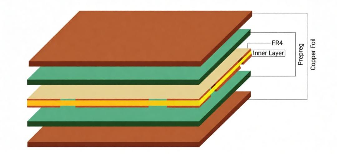
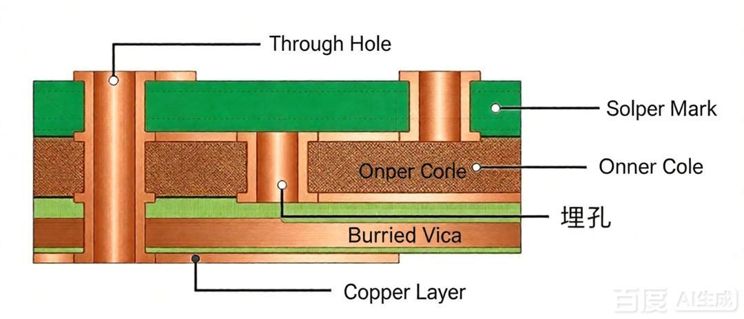
    (I)PCB (Printed Circuit Board) A PCB is a basic carrier used to support electronic components and enable electrical signal communication. Conductive copper lines are formed on the surface of an insulating substrate through processes such as etching, electroplating, and lamination. It forms the underlying framework of all electronic hardware.


    A PCB is composed of alternating layers of core, copper foil, and prepreg.


    1. Core Board:

    The core board is typically a rigid substrate with copper clad on both sides, providing conductive layers and structural support.

    The basic framework is an epoxy resin glass cloth insulating substrate (FR-4 is the mainstream). A layer of copper foil is completely laminated to both sides of the substrate. It comes pre-installed with double-layer conductive copper layers, allowing for separate etching of inner layer circuitry and power/ground copper foil.

    2. Copper Foil:


    Copper foil is a thin sheet material with copper as its main component, possessing excellent electrical conductivity, thermal conductivity, and ductility. Copper foil is the core carrier of conductive lines on a PCB, serving as the main channel for electrical signals to pass through the PCB and reach mounted components.
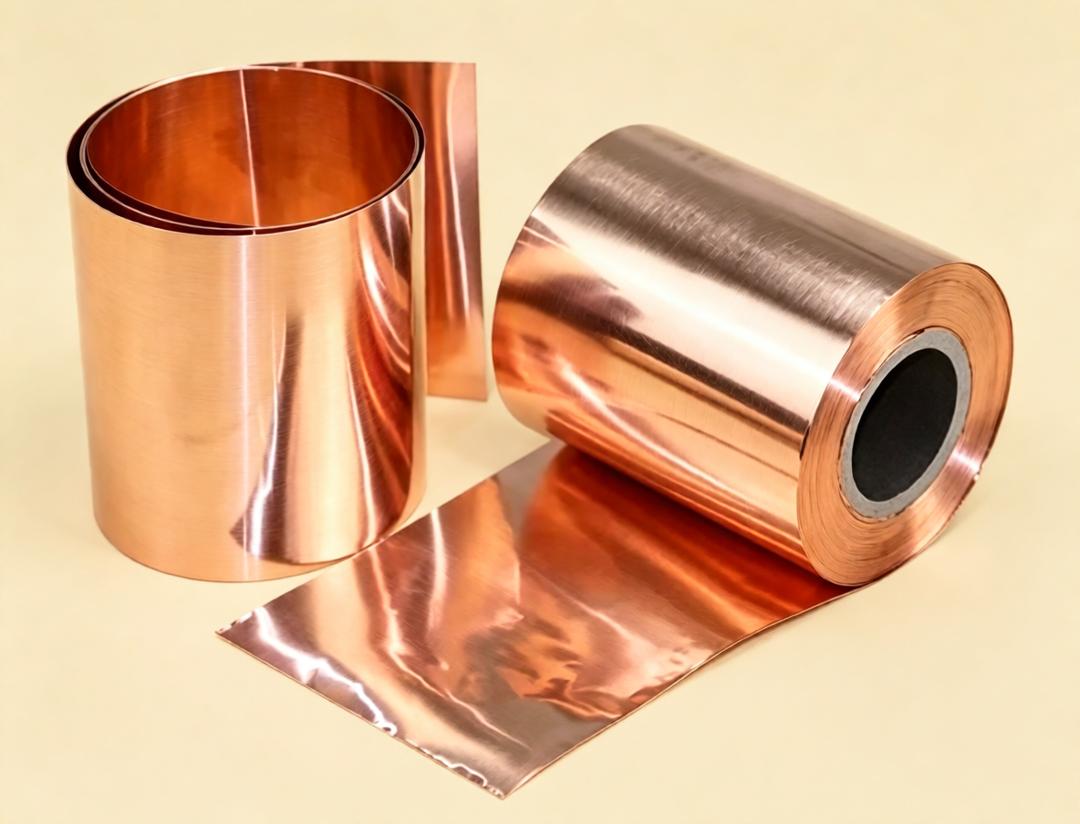


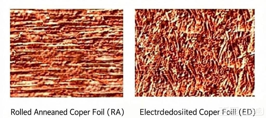
    Based on manufacturing processes, copper foil is mainly divided into two categories: electrolytic copper foil (ED) and rolled copper foil (RA).

    Electrolytic copper foil (ED): One side is smooth and the other is rough. The rough side is bonded to the substrate. It is suitable for rigid PCBs and has the widest application. Its cost is lower than that of rolled copper foil.

    Rolled copper foil (RA): The surface is smooth and flat with low roughness. It is suitable for rigid-flex PCBs, flexible circuit boards, and PCBs for high-frequency signal transmission. Its cost is higher than that of electrolytic copper foil.

    Request PCB Manufacturing & Assembly Quote Now


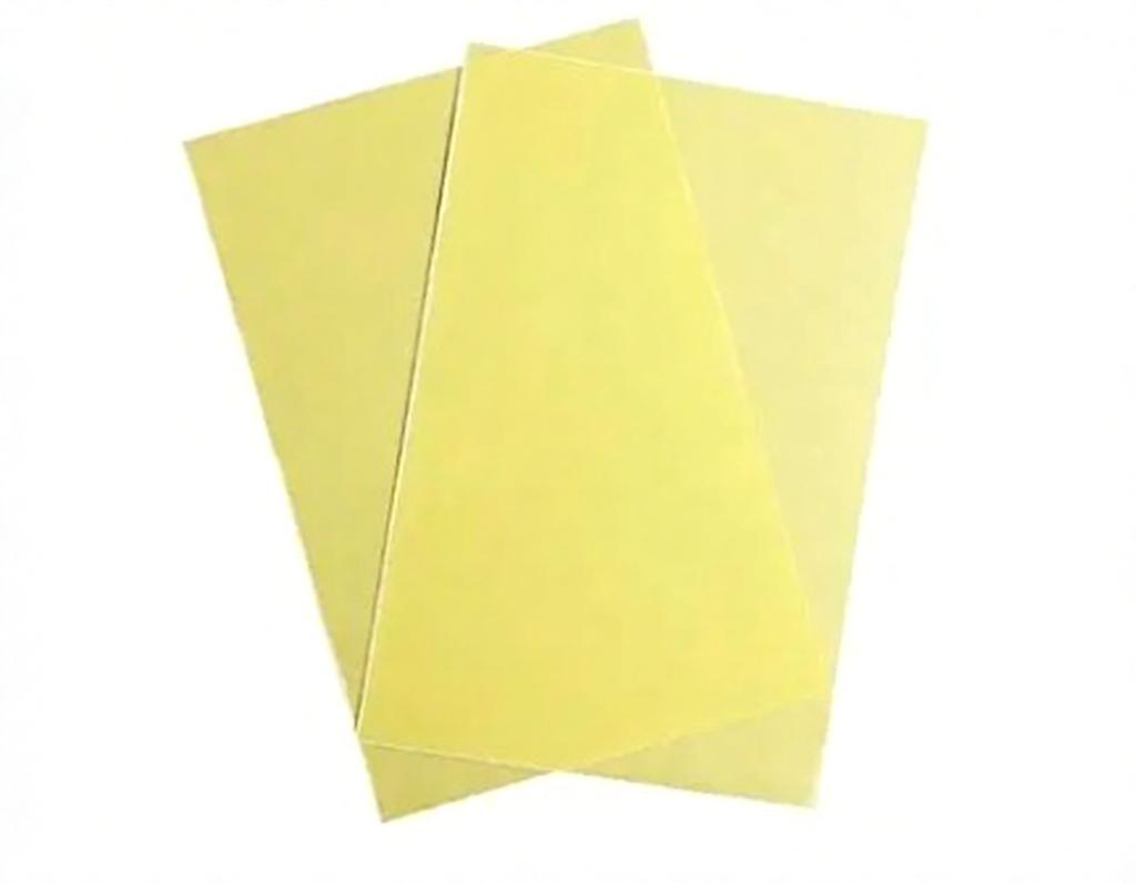
    3. Prepreg:

    Prepreg is the bonding material used in the lamination of multilayer PCB boards. It mainly consists of fiberglass cloth, resin, curing agent, accelerator, solvent, and filler. During lamination, the resin flows and cures upon heating, bonding the copper foil layers and inner core boards together while also providing interlayer insulation. The most commonly used resin is epoxy resin, but other resins include BT resin, CE resin, PPE resin, and polyimide resin (PI).
    4. Solder Mask:

    Solder mask is a permanent, heat-resistant insulating protective layer coated on the surface of PCB copper foil. Its function is to selectively cover non-soldering areas to prevent solder bridging and short circuits during soldering, and to protect the copper foil from oxidation, corrosion and physical damage.
    5. Other Auxiliary Materials


     Gold Salts (e.g., potassium gold cyanide) Key chemicals providing the gold ion source in immersion gold/gold plating processes, used to deposit a gold layer on the PCB surface.

     Dry Film (Photoresist Dry Film)
    Dry film is a photosensitive polymer material used in the PCB pattern transfer process to protect specific areas of the copper foil (ultimately forming circuit traces and pads), acting as an anti-plating and anti-etching agent.

     Working Principle: The dry film undergoes a polymerization reaction under ultraviolet light irradiation. The unpolymerized portions (containing hydroxyl and ester groups) dissolve in an alkaline solution, thus achieving pattern transfer.

     Structural Composition: Dry film consists of three layers—a polyester film, a photoresist film, and a polyethylene protective film.

     Difference from Wet Film: Dry film and wet film are two different types of photoresists. The choice depends on factors such as precision requirements, cost budget, and production efficiency. Dry film has higher resolution and is suitable for fine circuit fabrication.

    (II) Electronic Components

    Electronic components are a general term for electronic elements and devices. They are the basic functional units that constitute electronic circuits and equipment, including resistors, capacitors, inductors, diodes, transistors, and integrated circuits.

    Electronic components are mainly divided into passive components, active components, connecting devices, and other devices that are difficult to classify.

    1. Passive Components
    These cannot generate or amplify electrical energy/signals themselves. They passively regulate the current, voltage, and signals in the circuit through processes such as consumption, storage, filtering, voltage division, and current limiting. They do not require an external power supply and do not possess signal gain or switching control capabilities. They mainly include resistors, capacitors, and inductors.

    2. Active Components
    These require an external power supply to operate. They can control current, amplify electrical signals, switch on and off, and perform processing operations. They can achieve energy conversion and signal gain, and are the core "control unit" of the circuit board for logic, driving, operation, and voltage regulation. They mainly include through-hole diodes, transistors, and integrated circuit (IC) chips.

    3. Connecting Devices: These are components that enable electrical conduction and mechanical connection between circuits, boards, external devices, and components and PCBs. They only transmit electrical signals/current and do not participate in signal processing or power conversion; they act as circuit "bridges." They mainly include: onboard surface mount connectors, through-hole terminals, and switch-type connecting devices.

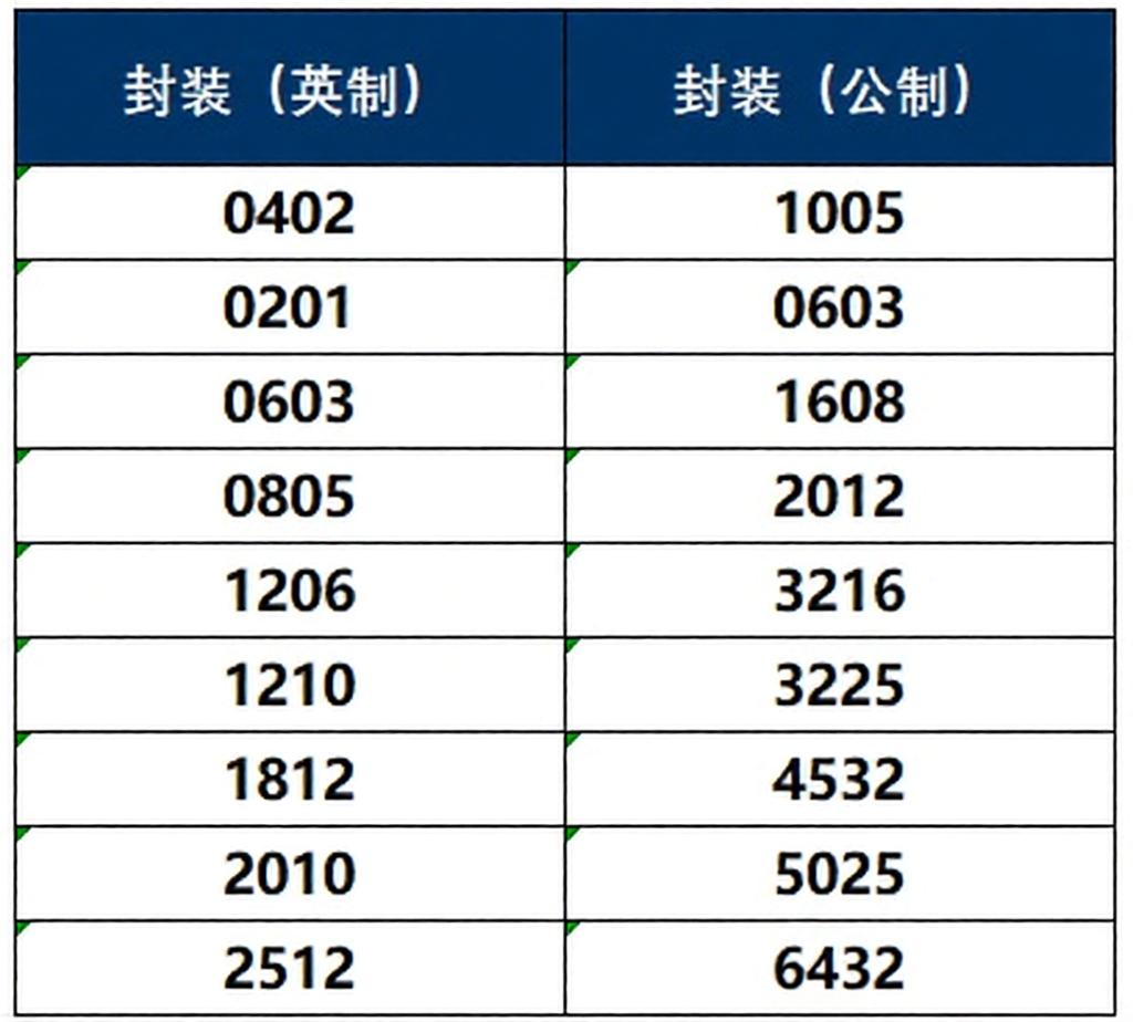
    The packaging mainly comes in two forms: imperial and metric, which can be converted to each other.


    (III) Solder Paste


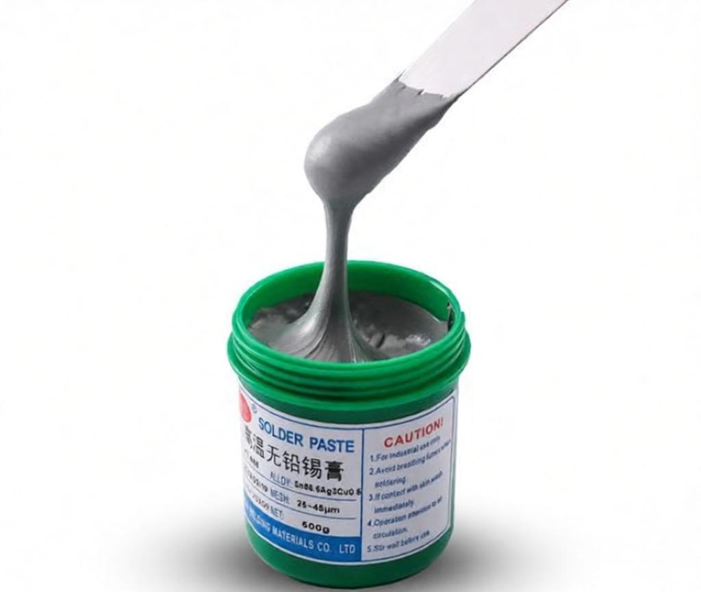
    Solder paste: A paste-like mixture containing solder powder and flux, printed onto PCB pads using a stencil. Classified by alloy composition and environmental standards, solder paste is mainly divided into leaded solder paste and lead-free solder paste.

    1. Lead-free solder paste:
    Main alloy composition: Tin-silver-copper (SAC305: Sn96.5/Ag3.0/Cu0.5), compliant with RoHS environmental standards, it is the mainstream choice for SMT manufacturing, mainly used in consumer electronics, communication equipment, medical devices, etc.

    2. Leaded solder paste:
    Main alloy composition: Sn63/Pb37 (eutectic), Sn62/Pb36/Ag2. Low melting point (approximately 183℃), good wettability, wide soldering process window, suitable for demanding industrial, military, and aerospace equipment, as well as old equipment repair.


    (IV) Auxiliary Consumables

    1. Stencil: Laser-cut stainless steel sheet (thickness 0.10~0.15mm), used as a "template" for solder paste printing
    2. Fixtures: Reflow soldering/wave soldering carriers, test fixtures
    3. Conformal coating: Moisture-proof, salt spray-proof, and mildew-proof coating material
    4. Cleaning agent: Water-based or semi-aqueous cleaning agent to remove residual flux after soldering
    5. Packaging materials: Vacuum bags, desiccants, humidity cards, and shock-absorbing cotton.


    Request PCB Quote Now


    II. Detailed Explanation of the Process

    (I) PCBA Process Flow

    The PCBA process flow is: Design and material preparation → SMT placement process → DIP insertion and wave soldering → Testing and quality control → Post-processing and packaging.


    (II) SMT Placement Process Flow

    1. SMT Production Line Layout

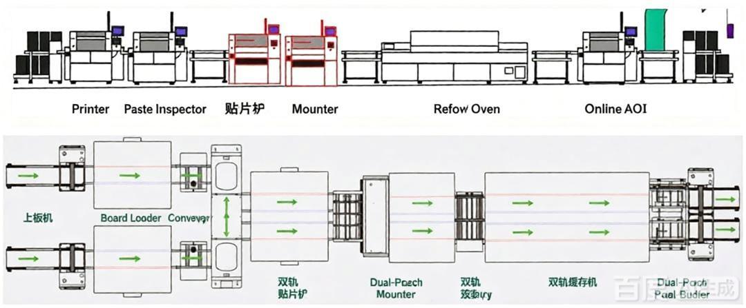
    The equipment in an SMT production line mainly consists of printers, solder paste inspectors, pick-and-place machines, reflow ovens, and in-line AOI equipment. The following diagram shows a common SMT production line layout.


    2. SMT Component Placement Process


    Pre-production preparation → Solder paste printing → SPI inspection → Component placement → Reflow soldering → AOI inspection → X-Ray sampling inspection → Cleaning → Board separation.

    (1) Pre-production preparation

    ① 100% dimensional inspection of the first batch of materials;

    ② Solder paste is warmed up for 4-8 hours + stirred for 2 minutes until the viscosity stabilizes at 180±20 Pa·s;

    (2) Solder paste printing

    ① Positioning: The PCB is placed in the printing machine carrier, and the optical positioning calibration reference point is used to fix the board;

    ② Soldering: The stirred solder paste is evenly spread on the stencil squeegee area;

    ③ Automatic printing: The equipment uses a double squeegee to uniformly transfer the solder paste through the stencil openings to the PCB pads;
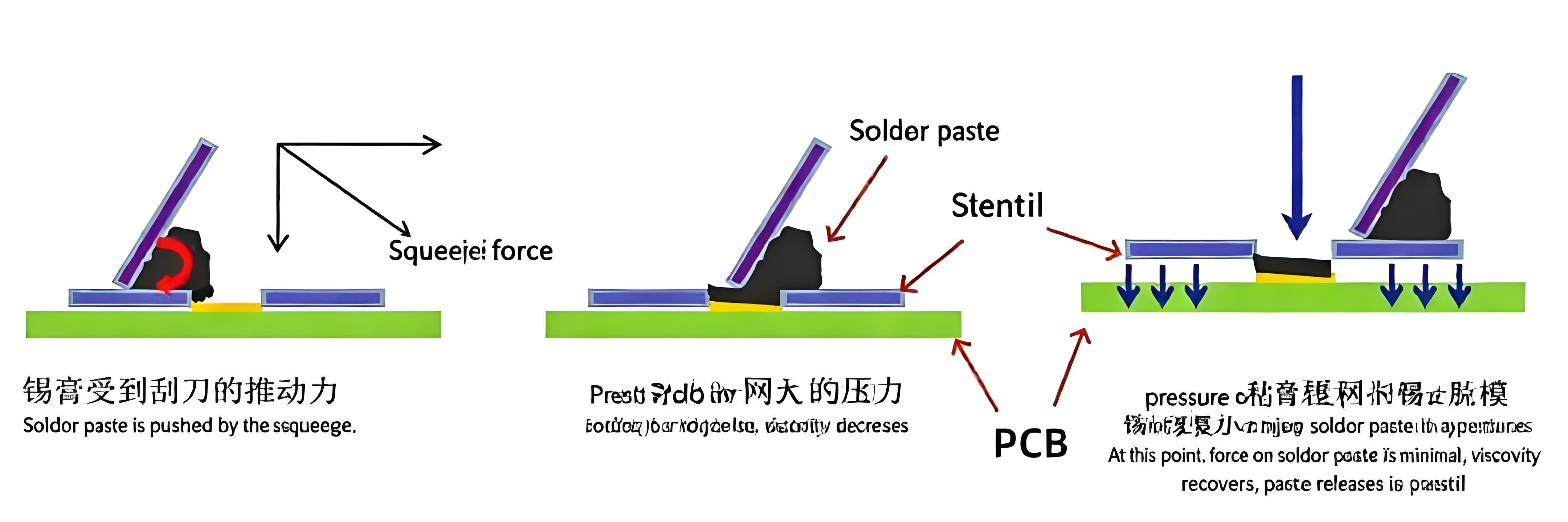


    ④ Demolding: After printing, the stencil is raised at a uniform speed to complete the solder paste transfer;

    ⑤ First Article Confirmation: After the first board is printed, the solder paste forming status is manually visually inspected.

    Precautions:

    (1) Too fast a demolding speed can cause solder paste spikes and insufficient solder; too slow a speed can cause solder paste accumulation and bridging;

    (2) Wipe the bottom of the stencil every 30 PCBs produced to prevent hole blockage;

    (3) Replenish with new solder paste every 2 hours of continuous production, with a new-to-old solder paste ratio of not less than 1:1.

    (3) SPI (Solder Paste Printing Inspection)

    ① Printed PCBs automatically flow into the SPI inspection station;

    ② A 3D laser optical camera scans all pads line by line, automatically collecting solder paste volume, thickness, area, and offset data;

    ③ The system automatically compares with standard thresholds to distinguish between OK/NG boards;

    ④ NG boards are automatically diverted to the rework station for manual wiping and reprinting; OK boards flow into the placement process. Precautions:

    ① The tension of the conveyor tape should not be too high to prevent components from flying or being thrown.

    ② Check the ejection box every 2 hours and calculate the ejection rate. If the ejection rate is >0.3%, stop the machine and check the materials and nozzles.

    ③ Clean the nozzles regularly. Blockage will cause pick-up deviation and missing parts.

    (4) High-speed placement

    ① Install trays, tubular, and reel precision materials (BGA/QFN/QFP) onto the multi-functional high-precision placement machine.

    ② Use dual vision cameras to synchronously image and align component leads and PCB pads.

    ③ Complete the placement of precision chips, connectors, and large-size ICs.

    ④ After the entire board is placed, it flows into the reflow soldering process.

    (5) Reflow Soldering

    ① The PCBs with surface mount technology (SMT) completed are continuously fed into a 12-zone reflow oven;

    ② Segmented heating: preheating zone → constant temperature zone → heating zone → peak temperature zone → cooling zone, following the RTS heating curve;

    ③ Solder paste melts upon heating, and the component pads and PCB pads metallurgically bond, completing the soldering process;
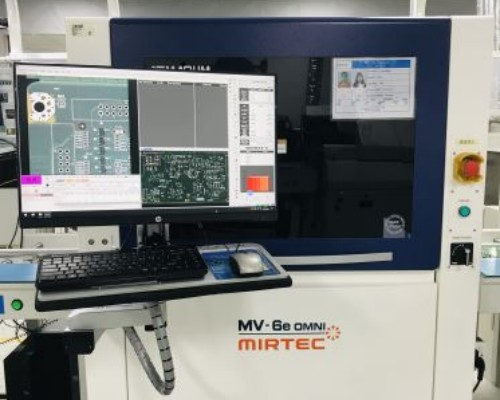


    (6) AOI Optical Inspection

    ① After soldering, the PCB automatically enters the AOI equipment, where dual cameras simultaneously scan the board surface;

    ② AI image algorithm identifies solder joint defects: insufficient solder, bridging, tombstoning, component misalignment, incorrect components, and missing components;

    ③ The system marks defective points, NG boards are diverted for manual re-inspection and repair, and OK boards flow into the next process. (7) X-ray Sampling Inspection

    ① Sampling is performed according to production batches, with 1 piece out of every 50 pieces selected for X-ray inspection; large-volume automotive boards undergo 100% full inspection;

    ② X-rays penetrate the PCB to image and observe the BGA and the solder joints hidden in the bottom shielding frame;
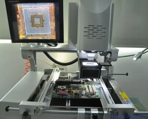


    ③ Software automatically calculates the percentage of void area in the solder joints and determines whether it is qualified according to the IPC-7095 industry standard; the void rate of the bottom solder joints of the BGA is the focus of inspection, according to the IPC-7095 standard, the first-level void rate is <15%.

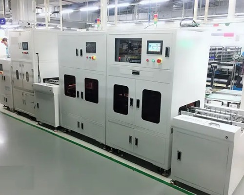
    (8) Separation

    ① Multi-panel PCBs are fixed on a milling cutter separation fixture;

    ② A high-speed milling cutter separates individual PCBs along the connection points between the boards, and a dust collection device is used to collect dust;

    ③ After separation, the board edges are manually polished to remove burrs, and all dimensions are inspected.
    (III) DIP Insertion Process Flow


    The main process flow of the DIP insertion process is: insertion → wave soldering → inspection. (1) Manual Insertion

    ① Manually insert the leads of through-hole components into the corresponding through-holes on the PCB according to the BOM;

    ② After insertion, gently press the components to ensure the leads are fully protruding from the board surface, without floating or reverse insertion;

    ③ Batch placement of PCBs with inserted components into a wave soldering fixture.

    Precautions:

    ① Polarized components (capacitors, diodes) must not be inserted in reverse; confirm the first piece before batch production;

    ② Avoid bending long-lead components to prevent damage to internal leads.

    (2) Wave Soldering

    ① The fixture holds the PCB and moves it at a constant speed through the flux spraying area, uniformly spraying flux onto the board leads;

    ② The preheating section heats up to activate the flux and remove lead oxidation;

    ③ The bottom of the PCB contacts the molten solder wave, immersing the through-hole leads in solder to complete the soldering;

    ④ Rapid cooling and unloading by air cooling.

    (3) DIP Visual Inspection
    Manual visual inspection of through-hole solder joints: no cold solder joints, missing solder joints, bridging, excessively long leads, or component misalignment. (IV) Testing Process Flow
    The testing process flow includes: ICT (In-Circuit Test) → FCT (Functional Test) → (Aging Test)

    ICT (In-Circuit Test): Using a dedicated bed of probes to contact the PCB test points, the soldering quality of components is checked, and electrical defects such as open circuits and short circuits are inspected to quickly screen out defective products.

    FCT (Functional Test): PCBs that pass the ICT test are powered on and run to simulate the actual working state of the product, verifying whether various functions such as voltage output and signal transmission are normal, ensuring that the finished product meets design requirements.

    Aging Test: For specific product requirements, the PCB is placed in a high-temperature environment and run continuously for 24 or 48 hours to expose early failures and eliminate potential defective products.

    ICT and FCT are mandatory tests; aging test is optional according to customer requirements. After passing the tests, the product proceeds to post-processing and packaging.

    (V) Packaging and Warehousing
    After passing the final inspection, the PCBA is placed in an anti-static vacuum bag, vacuum-sealed, and a desiccant and humidity indicator card are added. The outer box is then labeled and stored for shipment.


    Request PCBA Now


    Inquiry Us


    Related Products

    aluminum PCB

    aluminum PCB

    heavy/thick copper pcb

    heavy/thick copper pcb

    Arlon high frequency PCB

    Arlon high frequency PCB

    TMM10 high-frequency microwave RF board

    TMM10 high-frequency microwave RF board

    How long purchase PCBAs from China?

    How long purchase PCBAs from China?

    HDI PCB Manufacturer-High Density Interconnect PCB

    HDI PCB Manufacturer-High Density Interconnect PCB

    Product Categories

    • PCBA
    • Rigid PCB
    • HDI PCB
    • Rigid Flex PCB
    • Flex PCB
    • High Frequency PCB
      • Rogers PCB
      • Isola PCB
      • Arlon PCB
      • Nelco PCB
      • Taconic PCB
      • Teflon PCB
      • Neltec PCB
    • Metal Core PCB
      • Aluminium PCB
      • Copper PCB
    • Ceramic PCB
    • Laser Stencil
    • Reverse engineering
    • Purchasing components

    Links

    Google.comBaidu.com

    内页左侧广告1

    Feedback

    Contact Us

    sales@key-pcba.com

    234123644@qq.com

    Commercial and Cultural Building, Community 11 of Tangwei,Fuhai Street, Bao'An District Shenzhen 518103 GuangDong China.

    WECHAT

    Copyright © 2016 KEY TECHNOLOGY(HK)CO. ,LIMITED All Rights Reserved.

    • Skype.
    • E-mail
    • Whatsapp
    • Inquiry