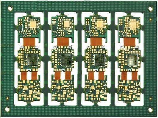
Description
Number of layers: 6 (RIGID), 2 (FLEX)
Size: 230 x 200mm
Board thickness: 2.0mm
Copper thickness: 1oz
Solder Mask: YES, Green, on both sides
Silk Screen: YES, on both sides
Board Finish:ENIG

The manufacturing process of rigid-flex PCB is as follows:
1. Punching: Drill holes on the FR4 circuit board and PP film. Note that the design of the alignment holes is different from that of general via holes. After punching, perform brown oxidation treatment.
2. Riveting: Stack the copper-clad laminate, PP film and FPC circuit board in order and then laminate them.
3. Laminating: This is a key step in the manufacturing of rigid-flex PCB. Stack the bottom copper-clad laminate, PP film, FPC flexible board and top copper-clad laminate in sequence and then laminate them.
4. Routing the board edge: Also known as removing the edge material, that is, removing the parts at the edge of the PCB circuit board that have no circuits and do not need circuits to be fabricated. Afterwards, it is necessary to measure the expansion and contraction of the material, because the PI used in the manufacturing of the flexible board also has expansibility and contractibility, which has a greater impact on the circuit board manufacturing.
5. Drilling: This step is the previous step of conducting the entire PCB circuit board. The manufacturing parameters need to be based on the design parameters.
6. Desmearing and plasma treatment: First use plasma cleaning to clean the via holes and the board surface to remove the smear generated by drilling.
7. Copper deposition: This is the process of electroplating through holes, also known as via metallization, to achieve electrical conduction of through holes.
8. PCB board surface electroplating: Partial electroplating of copper on the upper surface of the electroplating holes is performed to make the copper thickness above the through holes exceed a certain height of the copper-clad board surface.
9. Outer dry film positive production: The same as the anti-etch dry film production process of the FPC flexible board, the circuit that will be etched on the copper-clad laminate is produced. After completion, conduct circuit inspection.
10. Graphic electroplating: After the initial copper deposition, graphic electroplating is carried out, and a certain electroplating area is achieved by using the current time and copper plating wire according to the design requirements.
11. Alkaline etching: Conduct alkaline etching.
12. Printing solder mask: This step has the same effect as the protective film of the flexible board, generally called printing green oil. Conduct inspection after printing.
13. Routing the cover plate open: Also known as opening the cover plate, that is, by laser cutting, the unnecessary areas on the hard board are removed to expose the flexible board.
14. Curing: This is a baking process.
15. Surface treatment: Including immersion gold, hot air solder leveling, OSP, immersion silver, immersion tin, gold plating, etc., which can prevent the circuit board from being worn and oxidized.
16. Printing characters/printing text: Print the positions of the parts to be assembled and some basic product information in the form of characters on the rigid-flex PCB.


