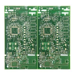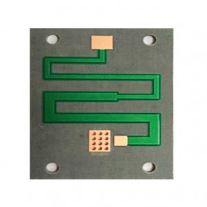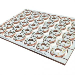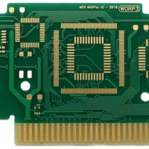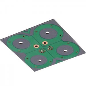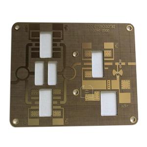
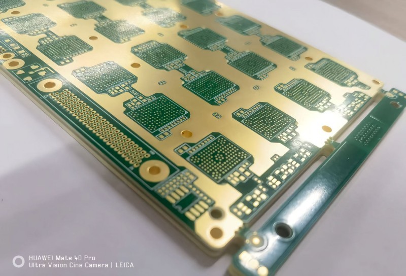
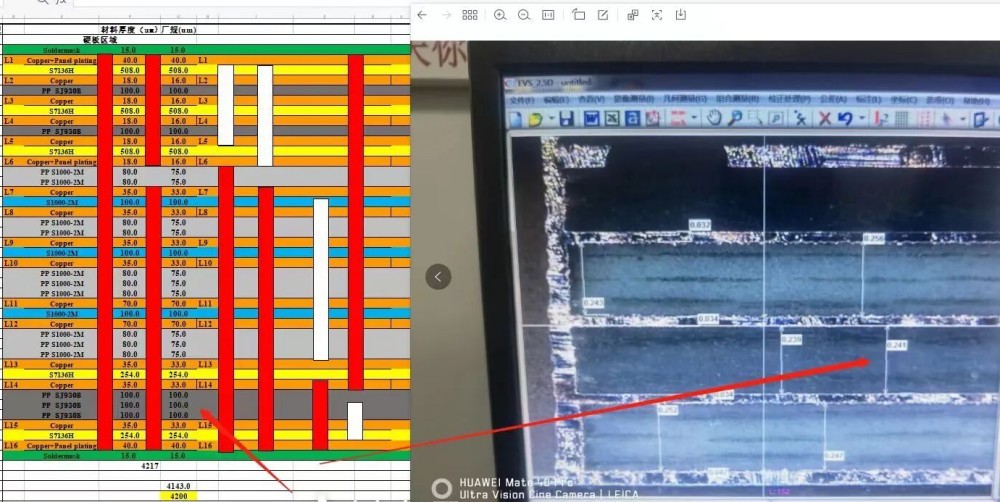
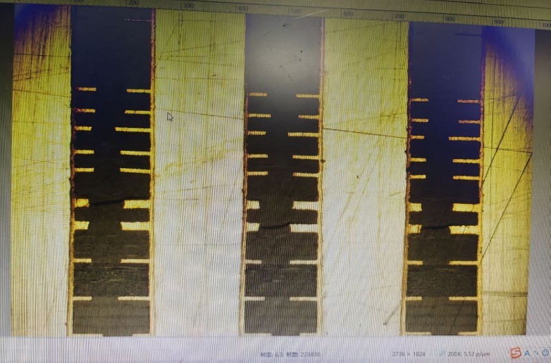
Layers: 16
PCB board thick: 4.2 ± 0.42 mm
Plate used: FR4+S7136H ShengYi
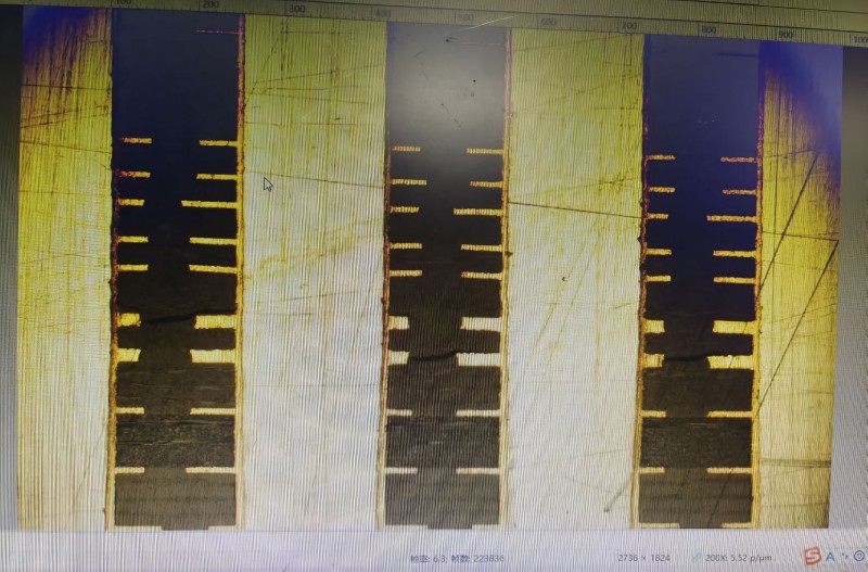
Minimum hole diameter: 0.1mm
Surface treatment: ENIG
BGA size: 0.25mm
Minimum trace width/distance: 0.1mm/0.1mm
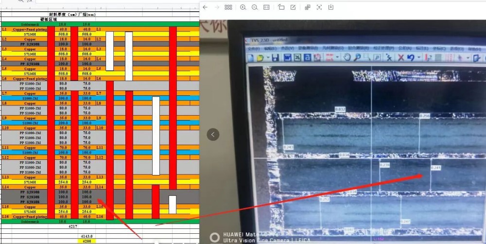
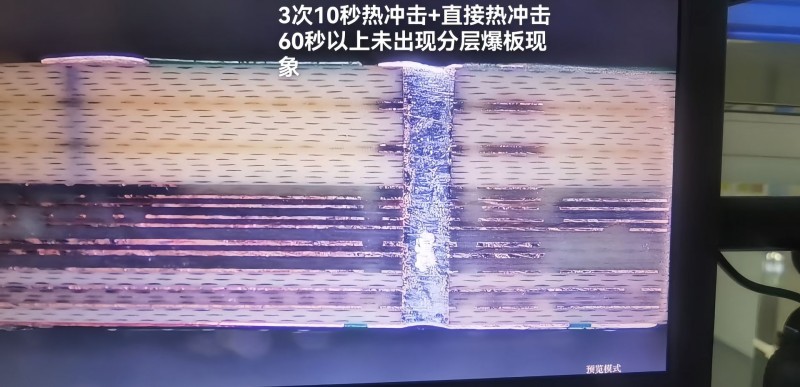
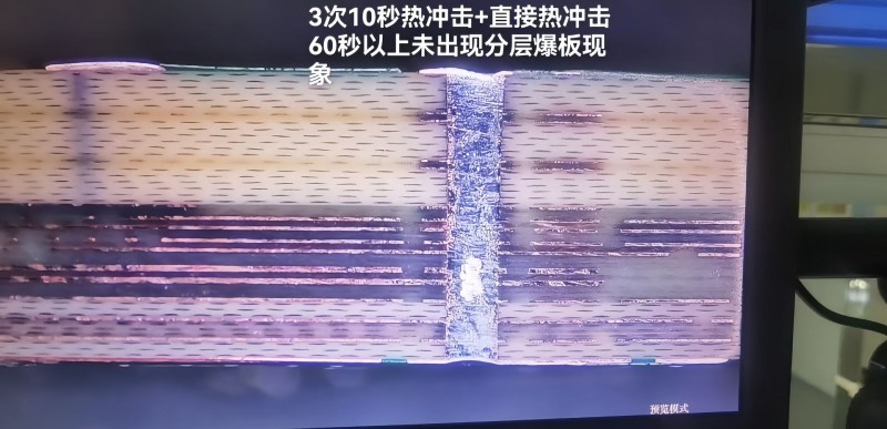
Blind+Buried hole structure
Process characteristics: HDI blind hole process, high BGA density, small spacing between hole to trace
Application field: RF
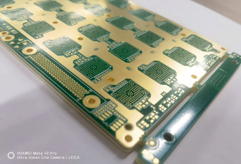
Stack-up specification