HDI PCB lamination is a core process in high-density interconnect (HDI) board manufacturing. Through multiple laminations, it achieves precise stacking of multi-layer circuits, a key technology ensuring inter-layer alignment accuracy and improving product yield.
I. Core Definition
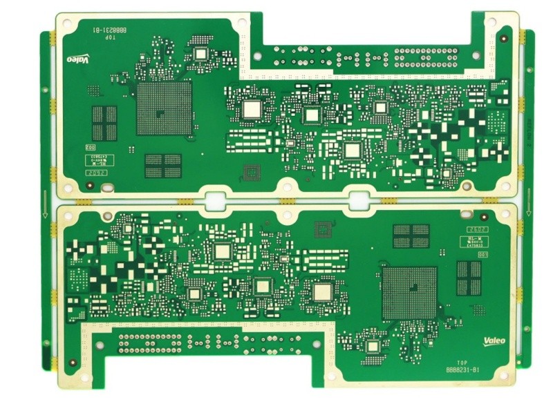
HDI PCB lamination, also known as sequential lamination, is a core process in HDI board manufacturing that uses multiple hot-pressing processes to sequentially bond inner core boards, prepregs, and copper foils to build a multi-layer interconnect structure. It adapts to the multi-stage stacking requirements of HDI from order 1 to higher orders, ensuring reliable connections between inter-layer circuits.
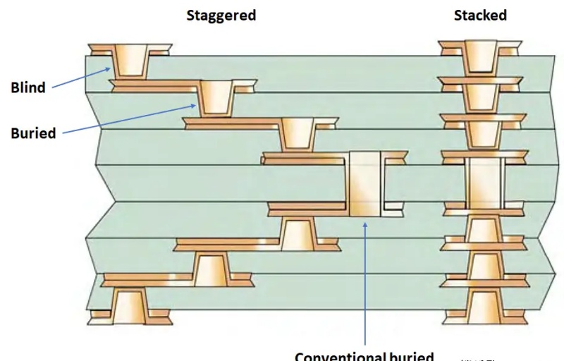
HDI PCB lamination process requires control of interlayer offset.
In HDI PCB lamination processes, controlling interlayer misalignment can be systematically implemented from multiple dimensions. The core is to stably control the misalignment within ±25μm or even higher precision, far exceeding the ±75μm standard requirement of IPC-6012C, ensuring high-yield mass production of multilayer HDI PCBs.
I. Pre-design Material Control: High Tg and low CTE core boards and prepregs are selected, with strict control over resin content and flow parameters to reduce deformation differences caused by thermal expansion and contraction.
A symmetrical stack-up design is adopted, with critical high-speed layers located close to the board center to avoid stress unevenness caused by mixing different materials. Misalignment trends are predicted in advance through process simulation.
II. High-Precision Alignment System Construction: CCD automatic optical alignment + X-ray drilling technology is used to unify the alignment reference onto the inner layer copper pattern, replacing the traditional mechanical hole reference and eliminating reference misalignment errors at the source.
LDI laser direct imaging technology is introduced to completely avoid pattern offset caused by film stretching, achieving alignment accuracy at the ±10μm level.
III. Optimization of Pressing Parameters
A multi-stage gradient heating-pressure control program is adopted, with the heating rate controlled at 2-5℃/min to prevent uneven resin flow from causing core board displacement.
The boards are pre-baked and dehumidified before pressing, and a high-parallelism vacuum press is used to reduce issues such as slippage and uneven local stress during pressing.
IV. Closed-Loop Management of the Entire Process
A database of board expansion and contraction is established. Before photoplotting, scaling compensation is performed on the X/Y axes of different layers to offset the expected deformation after pressing.
AOI and X-Ray inspections are configured for each key process. SPC is used to statistically analyze offset data and adjust process parameters in real time to achieve closed-loop control of "measurement-analysis-compensation".
Below is a table of applicable HDI interlayer offset control parameters, covering industry-standard parameters and core control indicators for different process stages.
Control Dimension
Key Parameter Item
Requirements for Conventional HDI Boards
Requirements for High-order HDI/AI Computing Boards
Control Purpose
Industry Basic Standard
Interlayer Alignment Offset (IPC Class 2)
≤75μm
-
Basic compliance for consumer/industrial grade products
Industry Basic Standard
Interlayer Alignment Offset (IPC Class 3)
≤50μm
≤25μm
High reliability requirements for military, medical, and high-end computing products
Material Control
CTE Matching of Core Board/PP Prepreg
Same-batch CTE deviation ≤ 2ppm/℃
Same-batch CTE deviation ≤ 1ppm/℃
Eliminate systematic deformation caused by thermal expansion and contraction
Material Control
Resin Content Tolerance of PP Prepreg
±3%
±2%
Avoid uneven resin flow pushing core board displacement
Alignment Process
Accuracy of Optical Alignment System
±15μm
±8μm
Reduce reference alignment error from the source
Alignment Process
Positioning Accuracy of X-Ray Target Hole
±20μm
±10μm
Unify the reference of inner layer pattern and drilling
Lamination Process
Heating Rate
2-5℃/min
1.5-3℃/min
Balance interlayer stress and reduce uneven shrinkage
Lamination Process
Lamination Vacuum Degree
≤5mbar
≤3mbar
Avoid local displacement caused by interlayer bubbles
Inspection Process
AOI Offset Detection Threshold after Lamination
≤60μm
≤30μm
intercept out-of-tolerance boards in advance, avoid waste in subsequent processes
Special Scene
Cumulative Offset of 24-layer Multi-order HDI
-
≤40μm
Ensure the alignment yield of stacked blind/buried vias ≥92%

Below is a detailed explanation of the HDI interlayer offset control parameters.


