Description
High‑Order HDI Any‑Layer Interconnection: The Core Hardware Technology for High‑End Electronic Products
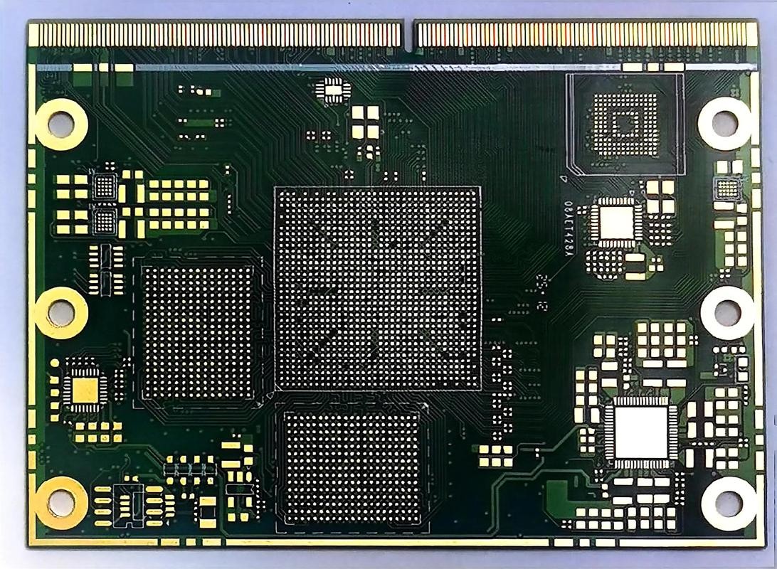
With the rapid advancement of consumer electronics and intelligent vehicle technology, flagship smartphones, automotive LiDAR, AI acceleration cards and other high‑performance electronic products are evolving toward ultra‑high computing power, ultra‑thin design and high‑speed signal transmission. The leap in product performance relies on breakthroughs in underlying hardware technologies. High‑order HDI printed circuit boards (PCBs) have become the core substrate for premium electronic devices, supporting the development and performance optimization of high‑end equipment. Among all key technologies for high‑order HDI boards, any‑layer interconnection (ALI) is the decisive factor determining PCB performance, precision and integration level, marking a critical divide between high‑end and conventional PCB manufacturing.
This revolutionary structural design delivers two major advantages for high‑end electronics. First, it significantly shortens signal transmission paths, reducing signal loss, delay and interference to fully unlock the performance of high‑speed chips. Second, it greatly improves wiring density, enabling more circuits and functional modules to be integrated within a limited board area. This supports thinner and more compact product designs and resolves the industry conflict between high performance and miniaturization.
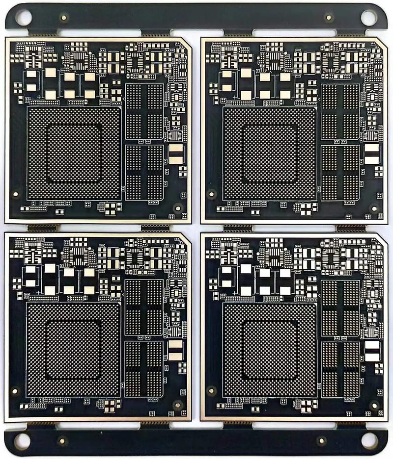
The implementation of any‑layer interconnection imposes extremely strict requirements on PCB manufacturing. Three core technical challenges must be overcome to achieve high‑density interconnection: microvia drilling, copper filling electroplating, and layer‑to‑layer alignment. Each process directly affects product yield and reliability.
Microvia drilling is the foundational step of ALI fabrication. Unlike standard PCB drilling, microvias for ALI typically have a diameter of ≤76 microns, too tiny for mechanical drilling. UV or CO₂ laser drilling machines are mandatory. During processing, laser power, pulse width and focal depth must be precisely controlled. Insufficient power causes residual adhesive or incomplete drilling; excessive power leads to carbonized via walls and distorted hole shapes, undermining subsequent electroplating quality.
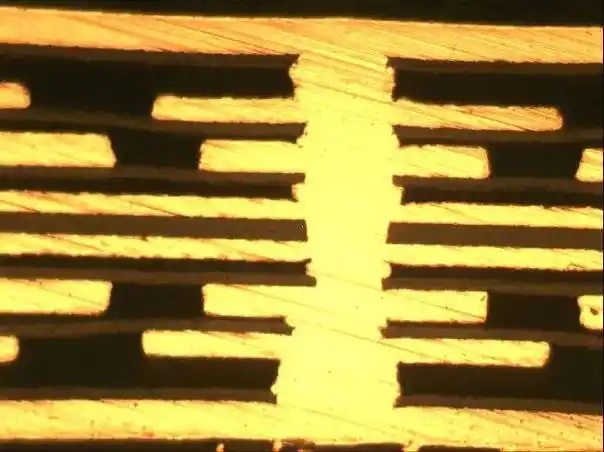
Following microvia drilling, copper filling electroplating ensures reliable inter‑layer conduction. Hollow microvias are fully filled with copper via electroplating. The process requires plating solutions with excellent throwing power and leveling capability, combined with precise pulsed current waveforms to promote bottom‑up void‑free copper deposition. The surface depression after filling must be controlled within 15 microns to guarantee flatness and subsequent assembly quality.
Layer‑to‑layer alignment is critical for multi‑layer PCB lamination. ALI requires precise registration between microvias and pads across laminated core layers. The overall alignment tolerance is within 50 microns, while via‑to‑pad accuracy must be below 25 microns. During high‑temperature lamination, PCBs expand and contract thermally, which may cause misalignment and result in electrical open or short circuits. Precise shrink‑swell compensation is therefore essential to maintain stable inter‑layer connectivity.
For terminal product developers, selecting a supplier with proven mass‑production capacity for any‑layer interconnection ensures three key benefits.
First, superior signal integrity. Shorter transmission paths and lower parasitic parameters minimize high‑speed signal loss and crosstalk, meeting high‑speed interface requirements of advanced chips and ensuring stable operation under heavy load.
Second, greater design flexibility. ALI relaxes routing constraints, allowing flexible arrangement of I/O ports and functional modules in limited board space. This facilitates product innovation and strengthens market differentiation.
Third, reliable mass‑production performance. Manufacturers capable of mastering the three core processes maintain mature engineering control systems and high production yields. This reduces trial‑and‑error risks and shortens product development cycles, accelerating time‑to‑market.
As electronic products continue to upgrade rapidly, high‑density, high‑precision and highly reliable interconnection solutions have become essential for next‑generation hardware development. If you are planning advanced high‑density interconnection solutions, please feel free to contact us (sales@key-pcba.com) for in‑depth technical discussion and customized support.


